Independent analysts have already noted that orders for Nvidia’s accelerator chips this year will require the use of 77% of all available silicon wafers of the corresponding class. Taiwanese sources now add that these same orders will load about 70% of the chip testing and packaging capacities using the advanced CoWoS-L method.
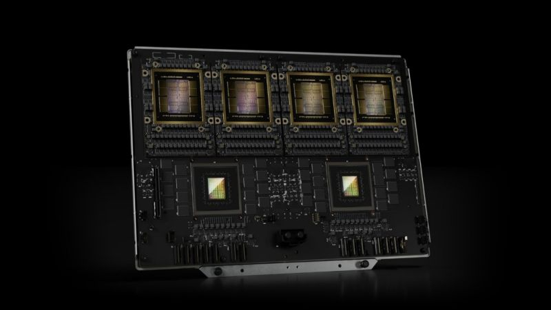
Image source: NVIDIA
This packaging technology is required for the production of Blackwell-generation chips, which are the basis of Nvidia’s advanced computing accelerators, as recalled by Economic Daily News. During this year, TSMC will increase its chip packaging capacity by at least 20% quarterly, which will allow it to process more than 2 million products of this type by the end of the year. In addition, additional demand may be created by orders from participants in the Stargate initiative in the United States, since the development of the national computing structure in this country will also require a decent number of Nvidia accelerators.
If last year, chip packaging services using advanced methods provided 8% of TSMC’s total revenue, this year they will exceed 10%, according to the company’s management. The expansion of Blackwell generation accelerator production will gradually reduce the need for representatives of the Hopper family (H100/H200), and the new generation will begin to dominate in the second half of the year.
In the near future, TSMC is reported to be making efforts to expand its eight CoWoS chip packaging facilities. Among them are two facilities acquired from Innolux, which previously produced display panels. In addition, TSMC has not yet decided on the location of two new CoWoS chip packaging facilities. As TSMC management never tires of noting, even the current rate of expansion of chip packaging capacities does not allow to cover the existing demand for these services. From the end of last year to the end of next year, TSMC plans to triple its chip packaging capacity.