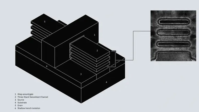
IBM and Rapidus prepared a report for the IEDM 2024 conference in which they reported progress towards mass production of 2nm chips. The partners have developed a method for producing both high-performance and low-power modifications of 2nm chips. Both technical processes are fully controllable and will be put into practice in Japan at the Rapidus plant by the end of the decade.

Image source: IBM
IBM began developing gate-all-around (GAA) transistors based on a stack of transistor channels made of nanopages more than 10 years ago together with Samsung. Then their paths diverged. Samsung began to independently develop the idea of GAA transistors, and IBM two years ago took on the Japanese company Rapidus, which was created as a Japanese response to TSMC, as a partner. The partners aim for Rapidus to become the center of global semiconductor contract manufacturing from 2027. This is quite possible if something irreparable suddenly happens to TSMC, and there may be a lot of changes in the Pacific region in the next five years.
When switching to the production of 2nm transistors, all manufacturers, including IBM and Rapidus, abandoned FinFET transistors. The transistor channels were returned from a vertical position to a horizontal one and were presented in the form of several levels of nanowires or nanopages located one above the other within a single transistor. The channels turned out to be nanostructures completely surrounded by gates. This made it possible to maintain operating currents, although the transistors themselves became even smaller.
The companies were faced with the challenge of mass-producing small transistors so that individual components were not contaminated by materials intended for others. IBM and Rapidus have largely overcome this problem, and also demonstrated the ability to produce GAA transistors with several threshold voltages in the channels: high for low-power electronics and low for high-performance electronics.
At the IEDM 2024 conference, IBM and Rapidus presented the technology for selective layer reductions – the space between n-type and p-type semiconductor channels. Depending on the thickness of this space, the threshold voltage will vary from higher to lower. The thickness is set at the transistor production stage and determines whether the chip will be productive or energy efficient. The partners presented two process options: SLR1 and SLR2. The SLR1 technology provides a high threshold voltage, and SLR2 – a low one.
Also, IBM and Rapidus were able to significantly reduce the contamination of the insulating substrate under the transistors with ions during plasma processing of chips during the production process – etching.
Kazuyuki Tomida, general manager of Rapidus US, also noted: “Multi-Vt [multi-threshold voltage] technology is a critical component of our nanopage architecture. The joint publication of this research paper with IBM Research at the IEDM conference represents an important milestone for Rapidus. This achievement strengthens our confidence in realizing our goal of manufacturing in Hokkaido at our advanced semiconductor facility, IIM.”