Three years after the appearance of the Alder Lake processors, Intel started a large update of the model range of desktop CPUs. At the end of last fall, she introduced Arrow Lake – new processors that have very little in common with Alder Lake and with their close relatives of Raptor Lake. And formally it was a very timely change of generations. The past processors of Intel Core on the 13th and 14th generations discredited themselves with a scandal with degradation, which greatly affected their reputation. And last year, AMD Ryzen 9000 and 9000x3D increased performance and in many cases began to look noticeably more attractive than the competitor solutions. In such conditions, Arrow Lake was entrusted with the role of a rescue circle, thanks to which Intel was going to correct her affairs in the desktop segment.
However, as you probably already know, nothing came of this: in some cases, Arrow Lake turned out to be even slower than their predecessors, so they can hardly claim high popularity and widespread. And this is quite strange. Compared to previous generations of Alder Lake and Raptor Lake processors, the new Arrow Lake made a serious technological breakthrough. Firstly, new P- and E-Jadra appeared in them, which are based on more progressive architectures. Secondly, Intel for the first time for the production of a mass product did not use its own production, but the power of a third-party contractor, TSMC, which can offer a more modern glass-conducting technology. And thirdly, Intel moved away from the use of monolithic silicon crystals in the desktop CPU, moving to the tyl (chiplet) structure of processors.
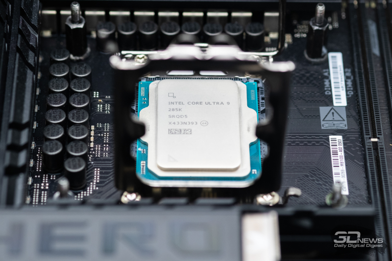
The official name of the new series of desktop solutions – Core Ultra 200 – is also chosen at all by chance. Representatives of the Arrow Lake family received so many innovations that Intel decided to make them a new reference point, and did not refer to the 15th generation of Core. Moreover, even if you look superficially at Arrow Lake, then its separation from Raptor Lake through the evolutionary staircase is equal to two and half steps. Between these processor families there is not only a full -fledged missed intermediate link – Meteor Lake, but also an half -hearted step in the form of the younger brother of Arrow Lake – the Lunar Lake processor. They ultimately did not get into the desktop segment: Lunar Lake was designed exclusively as a mobile product, and the release of the desktop version of Meteor Lake was converted by Intel along the way. Nevertheless, in each of these designs, Intel added and honed certain innovations and improvements.
TSMC N5
TSMC N5P
Although the senior Arrow Lake processors retained the same 8p+16e nuclear formula, which was inherent in their predecessors, it seemed that they should provide a noticeable leap in speed. Intel has repeatedly boasted its new Lion Cove architectures (P-Jadra) and SkyMont (E-Yadra), which provide a serious increase in IPC (specific performance in terms of the tact frequency). The company itself gave a +9 % estimates for P-nuclear and +32 % for E-yader, which, subject to the main level of the general clock frequency, could make Arrow Lake at least 15-20 % faster than its predecessors. In addition, it was also a serious improvement in energy efficiency: marketing materials stated that Raptor Lake achievement of Arrow Lake processors requires twice less energy, and in real applications they surpass them in terms of economy up to 40 %.
In this article we will analyze how these expectations diverged from reality, and most importantly, why this happened. The main character today will be the senior model in the new family – the 24-core Core Ultra 9 285K. However, in many cases, everything said will apply not only to him, but to all his brothers. And to make the analysis as substantiated as possible, we will talk not only about performance and power consumption in real tasks, but also about the technical features of Arrow Lake – the design, architecture, the new LGA1851 platform, and so on.
⇡#Arrow Lake lineup
The first part of the Arrow Lake lineup was presented on October 25, 2024. It consisted of five processors: the flagship Core Ultra 9 285K and its simplified modifications Core Ultra 7 265K and 265KF, as well as the more affordable Core Ultra 5 245K and 245KF (versions with the F index, as before, do not have a built-in GPU). All of these processors are based on the same silicon, and the differences built into them are artificial, but not insignificant. The differentiating features are the number of activated computing cores, cache memory sizes, frequency and thermal package.
In the first days of the new year, ordinary models aimed at the mass market were added to the top five K- and KF-processors. They have locked multipliers, lower frequencies and a more modest thermal package. See the table below for details.
P-cores, GHz Frequency
E-Jader, GGCGRACHIC,
Cores XeL3-cache,
Here it is immediately apparent that the maximum clock speed of Arrow Lake processors is limited to 5.7 GHz. This is significantly lower than the frequency that Raptor Lake processors once managed to reach. For example, the flagship Core i9-14900KS can be overclocked at nominal speed to 6.2 GHz, which is not available to new products. Moreover, the lag in frequency is not unique to the flagship. Other models are also inferior to their predecessors in terms of maximum frequencies by 100-200 MHz.
At the same time, the passport restrictions on maximum power consumption for the older representatives of the Core Ultra 200 series remained almost at the same level as for Raptor Lake. The maximum electrical power of the K-versions of Core Ultra 9 and Ultra 7 is 250 W (was 253 W). But for the Core Ultra 5 245K/KF it decreased from 181 to 159 W, and for the remaining Core Ultra 5 – from 148-154 to 121 W.
Otherwise, Arrow Lake’s numerical characteristics are similar to those of Raptor Lake. At this stage of processor evolution, Intel did not change either the established number of processor cores or the size of the third level cache.
⇡#Arrow Lake – a cost-effective processor with an AI accelerator
One of Intel’s primary goals when designing Arrow Lake was to curb power consumption and heat dissipation, indicators that have been steadily increasing in the company’s desktop products in recent years. Of course, the consumption of any processor can be limited by a strong-willed decision, but in this case performance will suffer. Therefore, in Arrow Lake there is no radical decrease in energy appetites – they are reduced exactly enough so as not to destroy the performance increase compared to their predecessors. However, the same P- and E-cores as in Arrow Lake are also used in mobile Lunar Lake with TDP in the range from 17 to 30 W, that is, new desktop processors can be very economical if necessary.
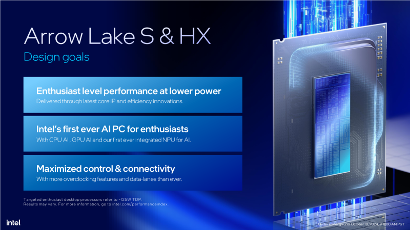
Another task that Intel solved by the release of Arrow Lake is the familiarization with the AI-Bomu. The company considered that the right moment for the emergence of mass platforms with a built -in neural -accelerator (NPU) came and added such an accelerator to a new desktop processor. However, the chosen approach was half a half. NPU in Arrow Lake is formally present, but it is very small in order to meet Microsoft formulated by modern PCs. This means that representatives of the Arrow Lake family will not provide hardware acceleration of the bulk of the ALGOGITMA in Windows 11, and the available NPU can only be used in some separate optimized tasks, the number of which can eventually be very insignificant.
However, the logic of Intel is that in the case of table processors, the transistor budget is more rationally redirected to traditional X86-Yadra, and the NPU in them is still prompted only for the box. And by the way, it was for this reason that the company did not focus on the ARROW Lake AIO in marketing materials, believing that they are not yet sufficiently developed for active promotion.
Otherwise, with the release of Arrow Lake, the company simply moved forward along an evolutionary path. The motto under which these CPUs entered the market is simple: “Cooler and more efficient mainstream processors for applications and games.”
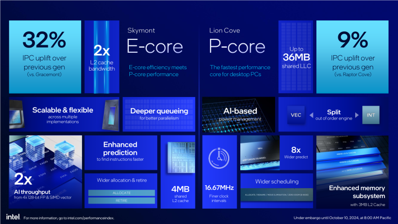
In short, the list of their main features (we will talk about each of them in more detail below) is as follows:
- Multi-chip processor assembled using Intel Foveros technology. It consists of four active crystals (CPU, SoC, GPU, I/O) and two passive crystals mounted on a single silicon substrate.
- All active crystals are manufactured by TSMC using EUV lithography processes and standards up to 3 nm. Their total area is 251 mm². The processor area on the substrate is 302.9 mm2.
- Up to 8 P-cores with Lion Cove architecture (+9% IPC compared to Raptor Cove according to Intel) and up to 16 E-cores Skymont (+32% IPC compared to Skymont).
- Support for Hyper-Threading technology has been removed from the processor at the silicon level for the first time since 2002.
- Second-level cache of P-cores is up to 3 MB per core (in Raptor Lake – 2 MB), E-cores – 1 MB per core (same as Raptor Lake). Level 3 cache – maximum 36 MB.
- The TDP of flagship models is 125 W, their maximum power consumption reaches 250 W. At the same time, a 30% improvement in energy efficiency compared to Raptor Lake is promised.
- Built-in graphics based on 4 XE nuclear baid with the Architecture XE-LPG (Alchemist). The number of executive devices in the graphic core compared to Raptor Lake is doubled.
- Hardware II-Processor NPU with a capacity of 13 TOPS.
- Dual-channel DDR5 is supported: up to DDR5-5600 (with UDIMMs) or up to DDR5-6400 (with CUDIMMs).
- PCIe 5.0 processor controller for 20 lines (you can use the PCIe 5.0 X16-video card and PCIe 5.0 x4-drive at the same time) plus additional 4 lines of PCIe 4.0.
- Thunderbolt 4/USB 4 in the processor.
- The new LGA1851 form factor: Arrow Lake is exclusively compatible with motherboards based on Intel 800 series chipsets.
- The processors belong to the Core Ultra 200 series.
⇡#Where did Hyper-Threading go, and what happened to Thread Director?
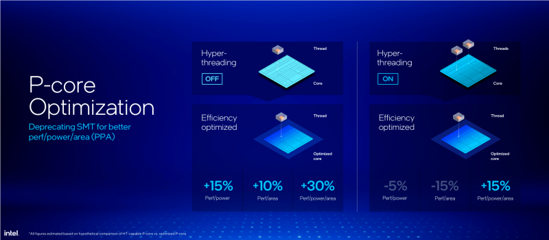
Arrow Lake relies on the new high-performance Lion Cove P-cores and efficient Skymont E-cores, which Intel first tested in Lunar Lake and which are two steps away from the Raptor Cove and Gracemont cores used in Raptor Lake. At the same time, the number of cores in the older representatives of the Arrow Lake family remained unchanged: there are again no more than 24 of them – up to 8 productive and up to 16 efficient. However, this does not stop Intel from promising that Arrow Lake outperforms Raptor Lake by 9% in single-threaded workloads and 15-20% in multi-threaded workloads due to architectural improvements. And this is especially surprising given the fact that Arrow Lake no longer supports Hyper-Threading multithreading technology, which allowed P-cores to execute two threads at once. That is, the new flagship with 24 cores supports only 24 simultaneous threads, while the Core i9-14900K is capable of serving 32 threads.
Performance degradation? Not really. Intel is selling the elimination of Hyper-Threading as if gamers have been asking the company for this for years, and now it’s finally listening to those requests. Of course, this is just an excuse. The real reason is something else, such as the desire to further limit the power consumption of new processors and reduce the area and transistor budget of the die. But the main thing that Intel draws attention to is that thanks to improvements in the architecture, the lack of Hyper-Threading will not be a problem in terms of performance, even when it comes to highly multi-threaded loads.
And he immediately explains: to compensate for the absence of Hyper-Threading in the Arrow Lake P-Yadrai, first of all, new E-Jaders should. Now it is a very powerful resource with a markedly increased performance, which, according to Intel, has approached the level of the Raptor Cove P-Jider. In addition, E-Jadram at Arrow Lake gave additional weight. To make them more significant, Intel has changed the principle of the distribution of flows-now all new flows are first sent to the E-Jadra, and only if their capacities are not enough, and the stream loads E-Yaro 100 %, its execution is transported to the P-Yadro.
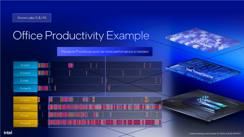
This means that in Arrow Lake, among other things, the strategy of Thread Director, the built-in software and hardware mechanism for load distribution, has changed. Along with the new cores, the third generation Thread Director appeared in Arrow Lake with different priorities. Not only does it initially favor efficient cores, but it also uses more advanced algorithms to classify tasks and predict their computing resource demands. For example, an important change to Thread Director is that it now tries to automatically separate gaming applications from all others, and use a different strategy for them, sending them directly to the P-cores.
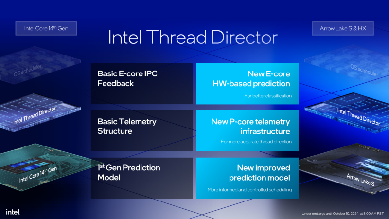
Intel claims that re-prioritizing thread allocation has further improved Arrow Lake’s cost-effectiveness. Threads that do not require maximum performance will be executed by E-cores, and resource-intensive applications will somehow end up being executed by P-cores, just with a slight delay. But the main thing here is that Arrow Lake has a significantly different performance profile – the performance ratio between P- and E-cores has undergone major changes. And this is easy to illustrate in a simple experiment involving the flagship Raptor Lake and Arrow Lake: the graph below shows the scaling of the result in the Cinebench R23 benchmark as the number of threads involved increases from one to the maximum possible.
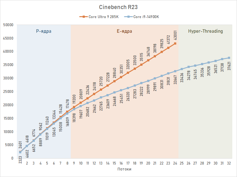
Since rendering requires maximum mobilization of resources from the CPU, both processors load the free P-cores first (one thread per core), after which the load is sent to the E-cores, and lastly the virtual cores provided by Hyper-Threading are used (if they are). Accordingly, in the range from one to eight threads, the lines corresponding to the Core i9-14900K and Core Ultra 9 285K are almost identical, and in the case of an eight-thread load, the gap reaches only 4%. This shows that Lion Cove P-Cores do not outperform Raptor Cove by too much. But the most interesting thing happens next. When the number of threads increases above eight, E-cores come into play. And if in the case of Raptor Lake, a noticeable break is visible in this place on the graph, associated with the lower power of its Gracemont E-cores compared to P-cores, then in the Arrow Lake curve such a break is almost imperceptible. It turns out that Skymont’s E-cores are really close in performance to P-cores.
Accordingly, the lion’s share of the gap between the Core Ultra 9 285K and the Core i9-14900K according to the Cinebench R23 results is formed precisely thanks to progress in E-cores. With a 24-thread load, the gap in test scores exceeds 30%, and Raptor Lake’s remaining eight threads, provided by Hyper-Threading support, are not enough to catch up with such a serious gap. As a result, with the highest possible multi-threading, the Core Ultra 9 285K outperforms the Core i9-14900K by 15%, which confirms Intel’s thesis that powerful E-cores are more useful than Hyper-Threading.
And the above graph shows how fundamentally Arrow Lake differs from the usual Raptor Lake. Therefore, we will have to devote part of this article to the architecture of the new kernels. This will help you understand how deep the differences between the new processors are.
⇡#Lion Cove Performance Cores
The lack of support for Hyper-Threading is not the only big difference between Lion Cove and the Raptor Cove nuclei used in Raptor Lake. Intel’s desire to raise performance, simultaneously improving energy efficiency, required a number of serious alterations, the most significant of which affects the change in the structure of the cache.
Thus, for the first time in the Lion Cove core, a “one and a half” level data cache appeared, located in the hierarchy between the L1 and L2 caches. This additional cache is 192 KB in size and, according to Intel, is in addition to the traditional 48 KB L1 data cache. However, the latency of the “one and a half” cache is twice as high as that of L1, and is 9 cycles, but in any case it will not be superfluous. Moreover, the traditional L1 cache in Lion Cove has become faster, and its latency has finally decreased from 5 to 4 clock cycles, as in Zen 4/Zen 5 cores.
On the side of increasing the efficiency of the data caching subsystem in Lion Cove, there is also an increase in the volume of the L2 cache, which in the new P-core has grown to 3 MB (versus 2 MB for Raptor Cove). At the same time, its latency has remained almost unchanged and is 17 cycles. True, to obtain this indicator, Intel had to reduce the associativity from 16 to 10 threads, which in theory reduces the efficiency of data caching (the probability of successful access).
In parallel with the growth of cache memory in Lion Cove, the DTLB buffer, which is responsible for quickly converting virtual memory addresses into physical ones, has also grown in size. Its depth has increased from 96 to 128 pages, which should have a positive effect on the efficiency of this buffer. But that’s not all. In an effort to speed up the work of the Lion Cove core with data, Intel added an additional, third addressable device to it, servicing upload operations.
But the improvements affect not only how data is processed in P-cores. Lion Cove’s execution pipeline has also changed noticeably across all of its stages to enhance the ability to process instructions in parallel. The loading of x86 instructions for execution began to occur at the rate of eight per clock cycle (and not six, as before), the rate of decoding of these instructions increased proportionally, and the micro-operation cache not only became larger by a quarter (up to 5250 entries), but also gained the ability to issue 12 micro-operations per clock cycle.
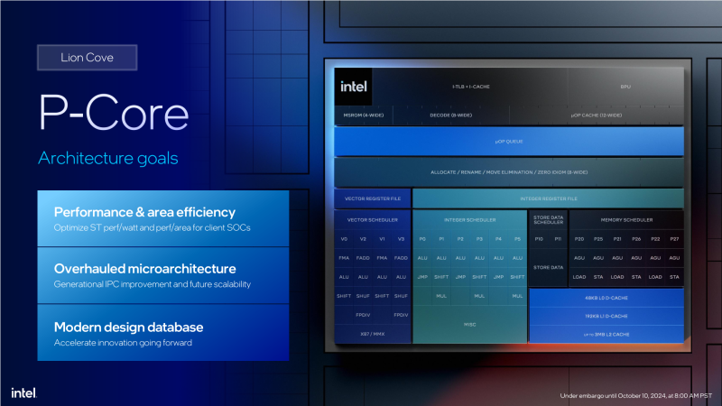
The Lion Cove executive domain not only acquired additional devices, but was strictly divided into integer and vector parts with its own schedulers. This separation will allow Intel, if necessary, to simply rebalance the core in future architectures. But what is more important at this stage is to increase the speed of the dispatcher to process eight micro-operations per clock cycle and the backoff buffer to twelve operations per clock cycle. Taken together with what was said in the last paragraph, this means that the Lion Cove core is capable of eight operations per clock cycle versus six operations for the Raptor Cove throughout the execution pipeline.
In order to support the increased pace of work, Intel upgraded the branch prediction unit so that it increased the volume of accumulated statistics by eight times and, as a result, became much more accurate. In addition, the depth of the instruction reordering buffer was increased by 13% and the number of ports in the execution domain was increased by one and a half times (from 12 to 18).
The increased computing power of the new core can be clearly seen from the increase in the number of actuators. The number of ALU blocks in the integer part of the executive domain increased from five to six, the number of address transition blocks – from two to three, shift blocks – from two to three, multiplication blocks – from one to three. Similar changes can be seen in the vector part. It now contains four SIMD blocks instead of three, plus two multiplication (FMA) blocks and two division blocks.
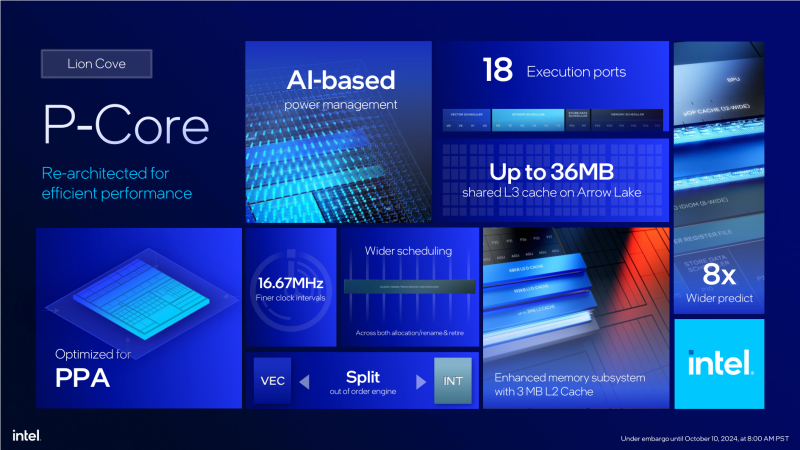
All this in total allows Intel to talk about improving the IPC indicator (specific performance at equal frequency) of new P-nuclear yaders by 9 % compared to Raptor Cove. In theory, such an increase is only partially able to compensate for the absence of Hyper-Threading technology in the P-Yadrachs, which allowed each nucleus to perform two streams in parallel. However, the support of Hyper-Threading at the architecture level still remained, but Intel decided to exclude it in mobile and desktop processors to reduce heat emission. And there is a certain meaning in this, since Hyper-Threading provided approximately 15 %increase in performance in multi-flow loads, but energy consumption increased by more than 25 %. At the same time, Intel promises to maintain Hyper-Threading support for server processors, since the advanced multi-fluidity in them is of key importance.
⇡#Effective SkyMont nuclei
Many people consider energy-efficient cores (E-cores) to be an afterthought in the processor that causes more problems than they are worth. However, this opinion does not apply at all to the E-cores in Arrow Lake. They use the new Skymont architecture, providing a noticeable leap in performance while maintaining low power consumption. And it is these cores that provide the lion’s share of the increase in the integrated performance of new processors as a whole.
Compared to the Gracemont E-cores used in Raptor Lake, the new Skymont cores have become significantly “wider”: their three-section decoder can process up to nine instructions simultaneously, which is one and a half times the capabilities of Gracemont. This expansion of the inlet part of the Skymont conveyor is reflected in all further stages.
In particular, the queue of decoded micro-operations now has a capacity of 96 elements versus 64 elements previously. In addition, the Skymont decoder uses a “nanocode” technique that avoids delays when interpreting complex x86 instructions. Each decoder section decodes independently, and they do not block each other’s access to shared lookup tables. This means that the rate of decoding in Skymont has increased not only due to the expansion of the decoder, but also due to the minimization of the number of forced downtime on complex x86 code.
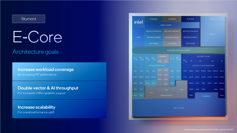
Further, the executive domain has changed proportionally. At the stage of renaming registers and placing commands for execution, eight micro-operations can be processed simultaneously (previously – five), and at the stage of resignation and completion – 16 micro-operations per clock cycle (previously – eight). A similar expansion of capacity also affected queues and buffers. For example, the instruction reordering buffer for out-of-order execution has grown to 416 entries (from 256), and similar changes also affect register files, a reservation station, and other auxiliary elements.
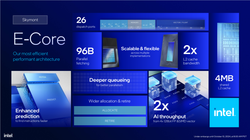
But what’s most impressive is how Skymont has grown in number of actuators. The number of ports is now increased to 26, and among other things eight integer ALUs, three branch processors and three data load devices are connected to them. As for working with real-number and vector instructions, for these purposes Skymont has four 128-bit ALUs with FMA (multiply-add) support. Based on this, we can say that the computing capabilities of the Skymont core have literally doubled compared to Gracemont.
A serious increase in the number of computing devices required a review of the kernel’s capabilities for working with data. As a result, the first level cache, although it retained the volume of 32 KB, received one and a half times higher bandwidth and learned to service three 128-bit data loads per clock cycle. In addition to this, the throughput of the L2 cache (and in E-cores it is shared by four cores at once) has doubled to 128 bytes per clock cycle. And in addition, the bus connecting the L2 and L3 caches has also expanded. Now you can pump up to 32 bytes per clock cycle through it. Along with the increase in throughput, the second level cache has also grown in volume – for every four Skymont cores there are not 2, as before, but 4 MB of L2. And in the new version of the E-cores, the L2 TLB (address translation table) has grown, which can now store up to 4 thousand entries, while previously it was 25% shorter.
It is curious that Intel itself is more willing to compare Skymont not with the E-cores of previous generations, but with the P-cores of Raptor Lake processors. According to the company, its new E-cores are quite comparable in specific performance to Raptor Cove (at the same clock frequency), but consume almost 40% less energy. At the same time, in a more traditional comparison with Gracemont E-cores, the IPC increase is 32% in integer workloads and up to 55% in floating point operations. Separately, Intel indicates that the speed of working with algorithms based on AVX and VNNI instructions has doubled. But at the same time, Skymont, like other E-cores of previous generations, does not support AVX-512.
However, speaking of E-Jader performance, you need to understand the following. Although in many indicators, for example, by the number of executive devices, the effective SkyMont nuclei exceed productive nuclei, they remain solutions of a different class and purpose. The fact is that the architecture of the E-Jader is developed with an eye for energy efficiency, and many important energy-intensive blocks, such as the branch of branches or cache blocks, are either reduced or abolished in principle. And this leads to the fact that E-Jadra copes with simple and straightforward score algorithms, but they are very much lost in productivity on a complex code with branches. P-Jadra in this sense is much more all-terrible, and therefore they retain the role of “heavy artillery” in resource-intensive calculations and continue to play the leading role in Arrow Lake, despite the increase in the role of E-Jader.
⇡#What is with IPC in practice
To get our own idea of the IPC increase of the new cores, we conducted a small test of their performance using microbenchmarks of the Aida64 package. In this test, we compared the results produced by the Core i9-14900K and the Core Ultra 9 285K by aligning all their cores at 4 GHz and activating either the eight P cores or the eight E cores exclusively.

And this test generally confirms most of Intel’s estimates regarding IPC gains. Thus, at an equalized clock frequency, the Lion Cove P-cores are almost 12% faster than the Raptor Cove P-cores – a pretty good result. However, it is only valid if you do not take into account the possibility of including Hyper-Threading technology in P-cores of the previous generation, which increases their multi-threaded performance by 17%. As a result, in the “Lion Cove vs. Raptor Cove with Hyper-Threading” comparison, the older P-cores come out as the winners – their advantage is about 4%.
Not everything is unambiguous and with a comparison of E-Jader. Intel is unconditionally right that the new Skymont E-Jadra is faster than the old Gracemont nuclei, and we were convinced that their superiority can really be estimated at 33 %. However, to put an Arrow Lake E-Jadra and P-Yadra from Raptor Lake, while clearly prematurely even at the same clock frequency. In our specific performance test, the new Skymont E-Jadra is lagging behind the performance from the old Raptor Cove P-Judas by significant 24 %.
The integral indicator presented in the diagram is calculated on the basis of ten benchmarks of a different nature, but in the results of individual tests you can also find a lot of interesting things. For example, it is clearly visible that in simpler integer algorithms, the gap between the P-Yadra and E-Jaders is really reduced, and may even disappear completely. But in difficult cases, where the share of code branches increases, and operations are carried out with numbers with a floating point of increased dimension, it can reach twice.


Another interesting point is that the Lion Cove P-core is not always better than the Raptor Cove P-core even without taking into account Hyper-Threading technology. There are tests, and they are not isolated, where the cores of the previous generation give better results than the new one. This is largely due to changes in the caching system and memory subsystem, and we will talk about this in a little more detail later.
⇡#Arrow Lake Tile Construction
Arrow Lake is the first multicristal desktop processor for Intel. Prior to this, the company sent exclusively monolithic chips such as Raptor Lake to the desktop segment. However, Arrow Lake inherits the approach used in the mobile Meteor Lake and Lunar Lake, where different functional blocks are spaced along various semiconductor crystals.
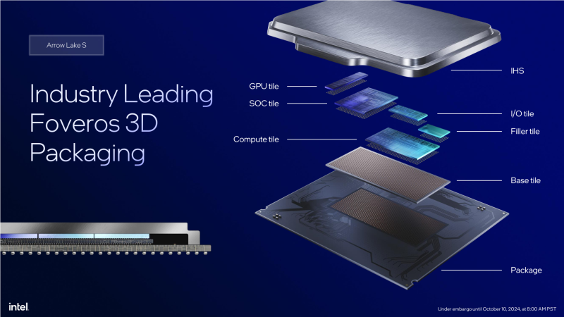
Such a distribution of roles through several chips allows Intel to save in production, since the most advanced processes are required for only one part of the CPU – computing tile (crystal with processor nuclei), which has maximum operating frequencies and heat emission. And in the case of Arrow Lake, this crystal is produced according to the 3-nm process for TSMC, which to a certain extent was a surprise, since initially Intel planned to release such crystals itself using its own Intel 20A process. However, at the last moment, the production was transferred to the external contractor, which led to a situation when all four functional tiles that make up Arrow Lake make TSMC.
The SoC crystal occupies a central place in Arrow Lake; a computing tile and an I/O crystal, which implements auxiliary interfaces (Thunderbolt 4, PCIe 5.0, etc.), are docked to it on one side, and a graphics tile on the other.
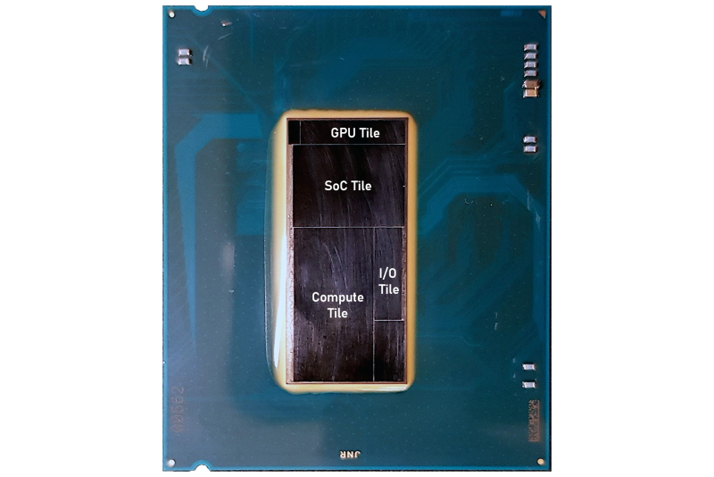
The connection of Tiles among themselves is based on Intel Foveros technology. This means that the four functional tiles are mounted on a crystal, inside of which all the intertetral compounds and the connection of crystals with the processor textual board are laid. The crystal substrate of Intel itself makes the Intel 16 process 22-nm, and it, like the entire processor in the collection, has an area of 302.9 mm2. This number is 20 % exceeds the “active” area of Arrow Lake, obtained by the addition of the area of functional tiles. This is due to the fact that two silicon dummies are also installed on the surface of silicon substrate, complementing the entire structure to the usual rectangular shape.
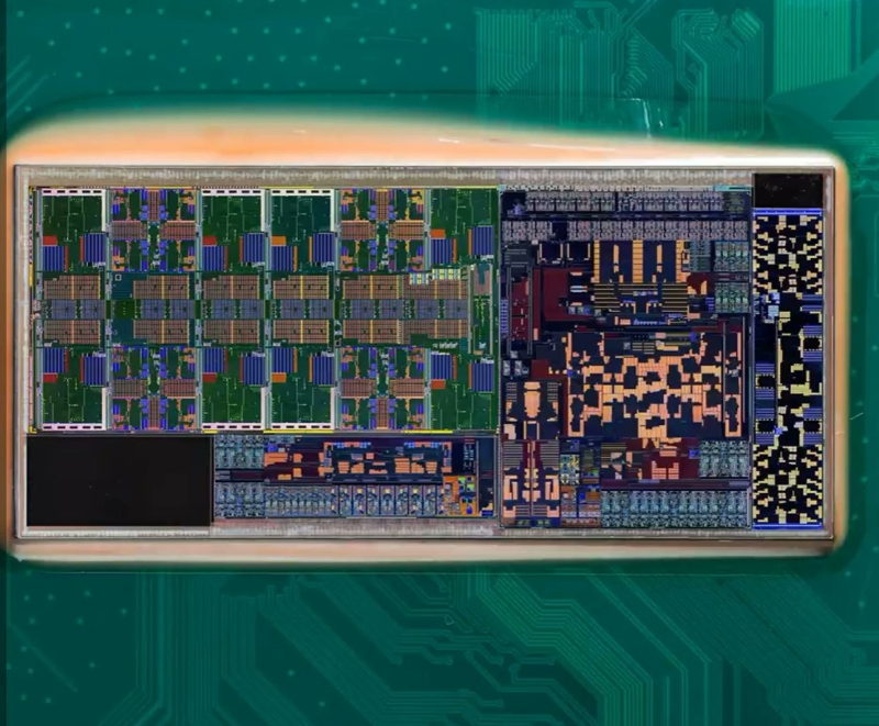
Assembling a multi-chip processor on a silicon substrate using Foveros technology is fundamentally different from AMD’s chiplet approach, when chiplets are installed separately on the processor PCB and are not connected into a single and almost monolithic silicon parallelepiped. Intel’s packaging technology is more interesting – it makes it possible to connect chips with a significantly larger number of conductors. As a result, the company was able to organize inter-tile communications with very high throughput, and, in theory, eliminate all bottlenecks when transferring data between Arrow Lake functional nodes located in different chips.
Indeed, the FDI (Foveros Die Interconnect) bus that connects tiles in the new CPUs provides a throughput of over 500 GB/s thanks to its 2048-bit width and operation at 2.1 GHz. For comparison, the Infinity Fabric bus, which AMD uses to communicate chiplets in its Ryzen processors, has a radically lower bandwidth – 64 GB/s. And this means that although Arrow Lake is assembled from several disparate silicon parts, they are connected to each other very tightly and efficiently.
⇡#Crystal CPU
The whole set of Lion Cove and Skymont nuclei is assembled in Arrow Lake in a separate semiconductor crystal (computing Tile), to which the third -level cache is also added to all of them. There are no more functional nodes in it, but this is not at all interesting in it, but the fact that Intel mixed the location of the P- and E-Jader- they no longer pile up inside the crystal with two clusters.
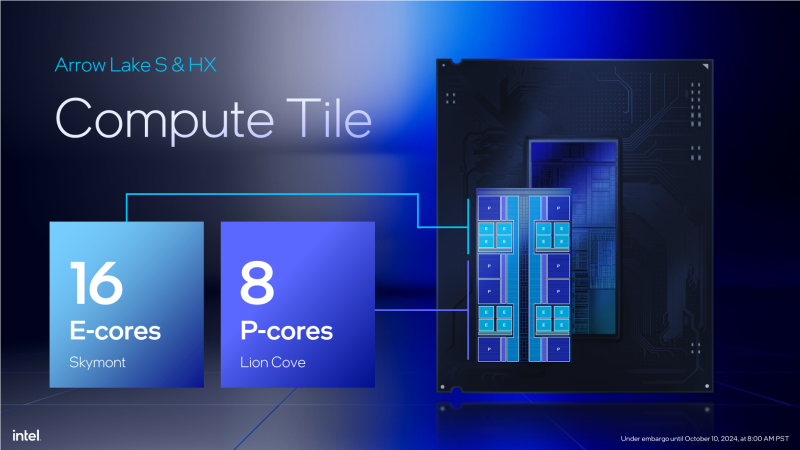
As an explanation, Intel talks about improved heat distribution across the silicon surface. And this makes a certain sense. Since the compute tile is manufactured at TSMC using the N3B process, even with 24 cores, the area is only 117.1 mm² – more than half the area of the Raptor Lake die. It is really difficult to remove heat from a small but hot die (AMD won’t let you lie), so Intel tried to place areas with high heat generation at a distance from each other. The most obvious solution to this problem is to scatter hot P-nuclei around the perimeter of the crystal. This is exactly what we see in the layout.
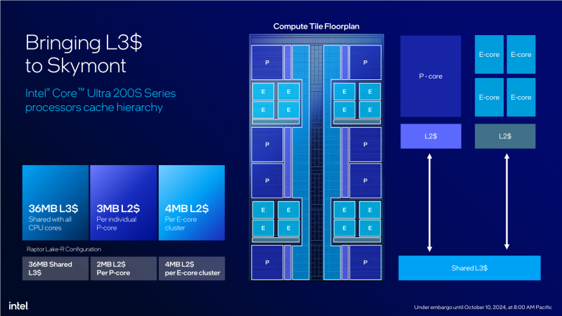
This distribution has another unobvious advantage. A reduced crystal with the nuclear formula 6P+8E, used in Core Ultra 5 processors, can easily be obtained from the maximum version of the crystal by simply truncation of some part of it. So far, Intel has not used this approach, but it is quite possible that with the spread of cheaper modifications of Arrow Lake it will begin to be used.
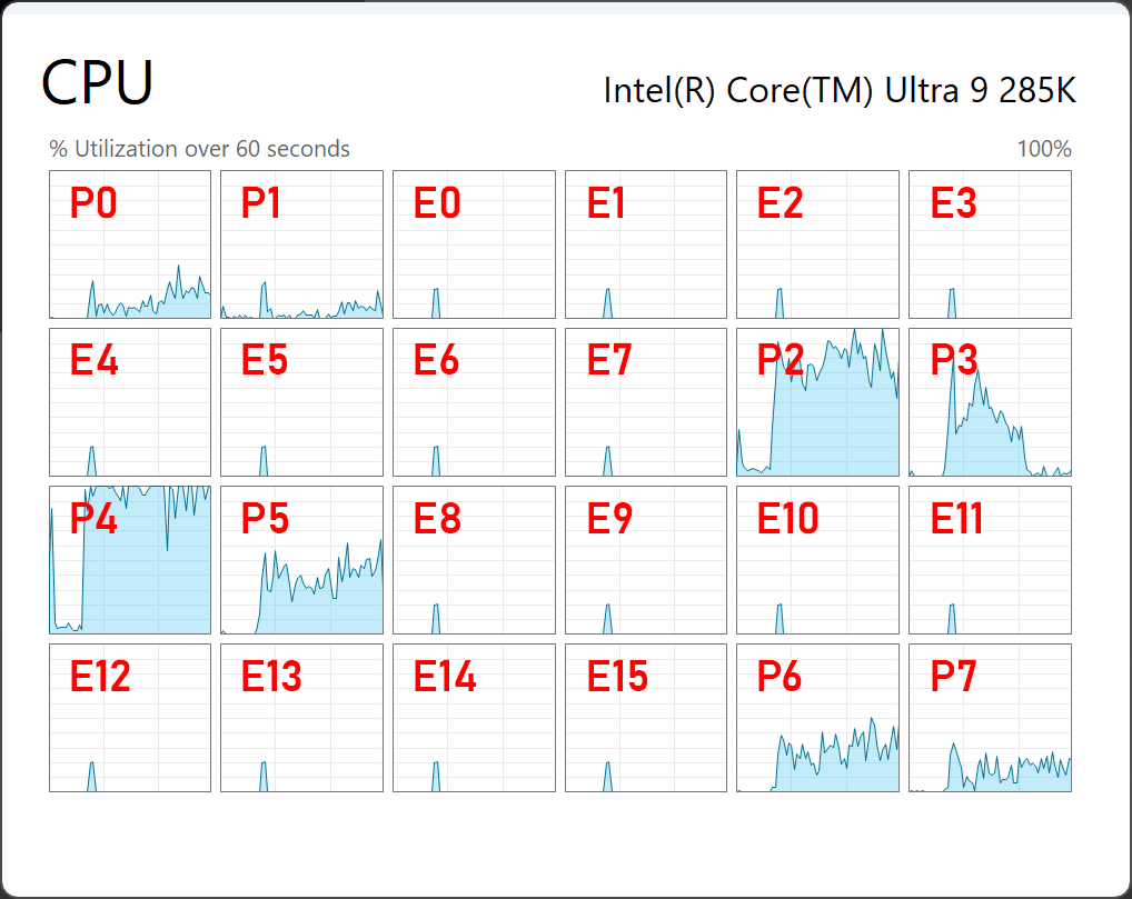
True, the ungrouping of P- and E-nuclei had an unexpected side effect – an unusual numbering of nuclei. For example, in the Core Ultra 9 285K, the productive cores are numbered 0, 1, 10, 11, 12, 13, 22 and 23. This means that it will now be much more difficult to recognize productive and energy-efficient cores in the performance monitoring in the Windows 11 task manager. I would like to hope that in order to avoid confusion, Microsoft will still figure out how to somehow divide the cores by their type.
The size of the L3-Kesha, permissible in the maximum versions of Arrow Lake, reaches 36 MB. As before, parts of this cache are distributed by 3-mults by blocks at the stop of the ring tire related to either the P-Yadra or to clusters of four E-Jader. Thus, there are no more than 12 such Kesha blocks of the senior Arrow Lake with a formula of 8p+16e. Core Ultra 7 processors with a 8p+12E formula similarly receive 10 parts of L3-Kesh, which gives its total volume of 30 MB. And the Core Ultra 5 with six P-nuclear and eight E-Jader can only count on eight L3-Kesh blocks with a total capacity of 24 MB.
This design of the third level Kesh-Mapamy makes it relatively slow in terms of delays, and this problem is aggravated with an increase in the number of nuclei connected to the annular tire. However, Intel is fighting her an increase in the second-level cache memory. Its total volume in Core Ultra 9, for example, reaches 40 MB, and in Core Ultra 7 and Core Ultra 5 is 36 and 26 MB, respectively. Thus, in Arrow Lake, Intel came to the fact that L2-Kesh overtook L3-Kesh. This was not there in the processors of previous generations.
You can see what the latency of the entire Arrow Lake cache memory subsystem in total looks like in the following graph, which shows the results of the Memlat test (in comparison with Raptor Lake).
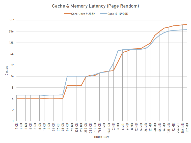
By adding a one-and-a-half cache and increasing the L2 cache, Intel actually achieved that when working with relatively small amounts of data (up to 8 MB), Arrow Lake has an advantage over Raptor Lake in terms of the speed at which they get processed into the cores. However, then the curves related to these processors change places, and the leader is the old Raptor Lake, the advantage of which becomes especially clear where all kinds of caches run out and accesses are addressed directly to memory. And this phenomenon deserves detailed discussion.
⇡#SoC and memory work
The second most important crystal of Arrow Lake, which largely determines its characteristics and features, is the SoC (system-on-chip). It is manufactured using the TSMC N6 technical process and contains three key components: a DDR5 memory controller, a PCI Express bus controller, and a neural network accelerator.
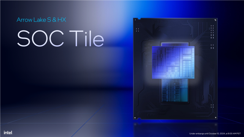
In addition, inside the SoC there is a media engine related to the built-in graphics core (which in Arrow Lake is implemented on a separate chip), as well as a unit responsible for display interfaces. The latest generations of mobile processors, for example, Meteor Lake or Arrow Lake-H, also contain a pair of energy-efficient LPE cores on the Crestmont architecture in the SoC, but desktop processors do not.
The PCIe controller built into Arrow Lake is notable for the fact that it supports 24 lanes—four lanes more than Raptor Lake. This allows you to connect directly to the processor only a video card in PCIe x16 mode, but also two drives in PCIe x4 mode. True, one of the PCIe x4 interfaces for SSDs is limited to only the fourth version of the protocol, but 20 lines out of 24 available work without problems with PCIe 5.0 devices.
As for the NPU hardware neural networks, it was added to the SOC on the principle of “to make it.” He cannot take some serious work on himself due to relatively low performance. But on the other hand, Intel got the opportunity to put in the specifications of Arrow Lake a box in the line “optimized for AI”.
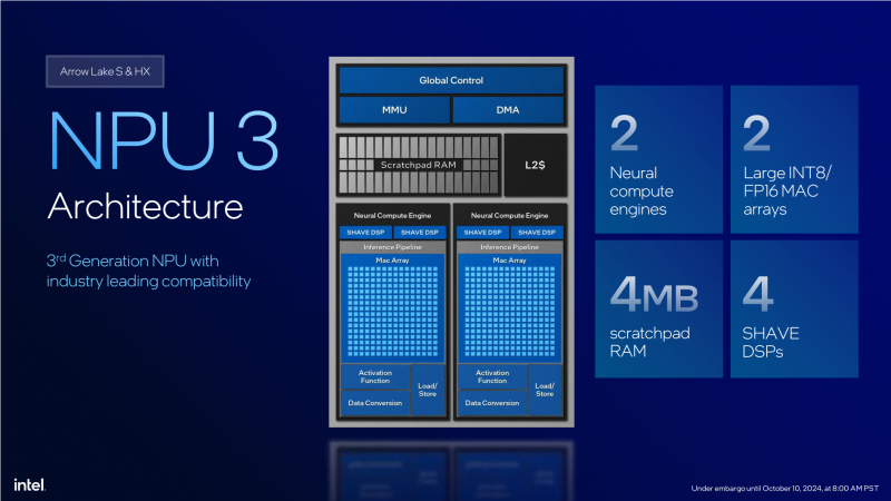
The theoretical power of this NPU is limited by 13 TOPS (trillions of eight-bit integer operations per second), and it is taken from Meteor Lake without any changes. Such performance is not enough to meet the requirements of Microsoft Copilot+ PC (40 TOPS), which means Arrow Lake will not be able to work with the bulk of Windows 11 and function, performed locally (primarily recall). Therefore, it is not surprising that, speaking of new processors for desktop systems, Intel tries to bypass the theme of NPU, especially since the previously published mobile Lunar Lake, the performance of the II-Processor is three and a half times higher.
But the DDR5 memory controller located in the SoC deserves much more close attention, since quite serious changes have occurred in it. In the new processors, Intel has raised the memory frequency bar, and now their characteristics include support up to DDR5-6400. At the same time, the Arrow Lake memory controller has lost backward compatibility with DDR4, which was preserved in the latest generations of Intel processors for quite a long time.
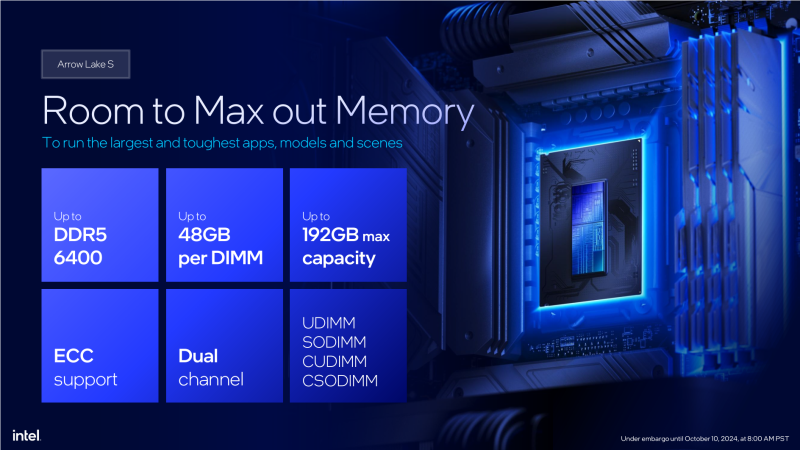
At the same time, there is one nuance associated with DDR5-6400 support. Based on official information, this regime requires compliance with some additional conditions. Firstly, formally it is only possible when using two peer-to-peer DIMM strips in the system. And secondly, its performance is guaranteed exclusively with CUDIMM modules, which are equipped with their own clock generator that improves signal synchronization. The maximum officially guaranteed mode available for conventional unbuffered UDIMMs remains DDR5-5600, which was also available in Raptor Lake.
However, all these memory requirements set forth in the official specification do not interfere with Intel to say that it is better to use as high-speed memory as possible with Arrow Lake, for example, DDR5-8000 (it even calls it “the best choice for enthusiasts”). Compatibility with it is not guaranteed by the specification, but as follows from the clarification of the company, the new processors received a significantly more stable memory controller compared to the one that Raptor Lake was equipped with, and most CPU copies should earn without problems with high -speed DDR5 modules, especially If these modules are Cudimm.
However, as it turned out in practice, the design of Arrow Lake is allowed an annoying miscalculation associated with the placement of the memory controller precisely in the SOC crystal, and not along with processor nuclei. The physical removal of this controller from its main users (computing nuclei) affected the performance of the memory subsystem sharply negatively. In the processors of past generations, the memory controller was connected to the ring tire actually directly, which made it possible to achieve when accessing memory and high throughput and low latent. Now, on the highways between the processor nuclei and the memory controller, another additional link arose – the FDI bus, responsible for the connection of the Tiles. And although this tire has a gigantic throughput, the problem lies in its operation at its own frequency of 2.1 GHz, which is not synchronized with the frequency of the ring tire of 3.8 GHz. This asynchronism causes noticeable overhead expenses when addressing memory, which in the processors of past generations were not in principle.
As a result of this, Arrow Lake, in terms of speed of working with memory, markedly lose the processors of the previous generation. Let’s take a look, for example, at the results of measurements of the metric of memory subsystem AIDA64 Cache & Memory Benchmark in Core Ultra 9 285K and Core i9-14900K when using the same DDR5-6400 modules with 32-39-39-102 timing.
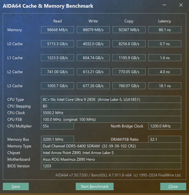
Core Ultra 9 285K, DDR5-6400

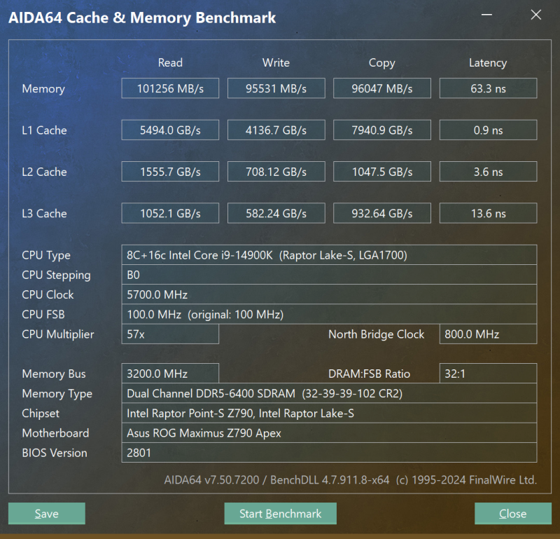
Core i9-14900K, DDR5-6400
In terms of memory bandwidth, the Core Ultra 9 285K and Core i9-14900K are almost the same – the FDI bus has almost no effect on this parameter due to sufficient bandwidth. But the difference in latency looks simply catastrophic. Arrow Lake’s latency is more than a third higher, and this can be a serious problem in memory-sensitive applications, which include many modern games.
As a consolation, we can only say that Intel has already realized its mistake, and in the next generation of processors (in Panther Lake) it is going to first return the memory controller to the same chip with the computing cores, and then (in Nova Lake) it will try to implement it on a separate chip in a new way, avoiding harmful tire desynchronization.
⇡#Built -in GPU
Intel usually does not provide its desktop processors with a powerful graphics core, redistributing the transistor budget in favor of computing capabilities. This same approach continues at Arrow Lake. The graphics in it are made in the form of a separate crystal (tile), produced using TSMC N5P 5nm technology, and this is the smallest crystal in size that is part of Arrow Lake.
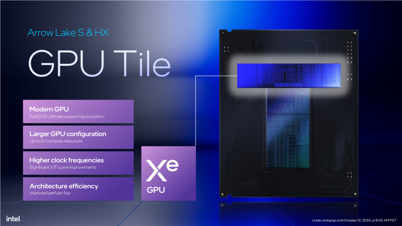
Moreover, the graphics core in Arrow Lake is based on the relatively older Alchemist generation architecture, not Battlemage, and only contains four Xe-LPG cores (which offer 64 execution units and 512 unified shaders). Thus, the integrated graphics of Arrow Lake desktops is inferior in theoretical performance to even the entry-level discrete graphics card Arc A310. In addition, Intel removed XMX tensor units from the built-in GPU. But even with all these limitations, Intel promises more than double the performance of the old Xe-LP graphics core on Raptor Lake desktop processors, plus full support for ray tracing and XeSS scaling, as well as DirectX 12 Ultimate compatibility.
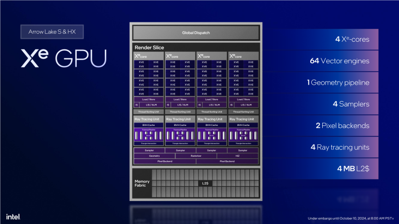
However, Arrow Lake graphics can hardly be considered seriously by anyone as a suitable option for building a gaming PC. It may only be interesting in office configurations that do not encounter gaming loads. In other words, users of systems based on Intel processors who care about graphics performance should, as before, focus on full-fledged discrete video cards.
But Arrow Lake received a pretty good media engine. It supports hardware accelerated video playback at resolutions up to 8K at 60 Hz with 10-bit color and can decode all modern formats, in particular, VP9, AVC, HEVC, AV1 and SSC. Hardware-accelerated encoding is supported for VP9, AVC, HEVC and AV1 formats and resolutions up to 8K@120Hz with 10-bit HDR. The graphics core is also capable of outputting images to four displays with resolutions up to 8K at 60 Hz, and supported connection standards include HDMI 2.1, DisplayPort 2.1 and eDP 1.4.
⇡#LGA1851 platform and Intel Z890 chipset
Together with Arrow Lake desktop processors, the new LGA1851 platform was released, in which they are supposed to be used. This means that to build a system based on Core Ultra 200, a new motherboard will be required. So far, all such motherboards are based on the Intel Z890 chipset, but this will change in the near future. More affordable system logic options in the form of B860 and H810 have already been presented.
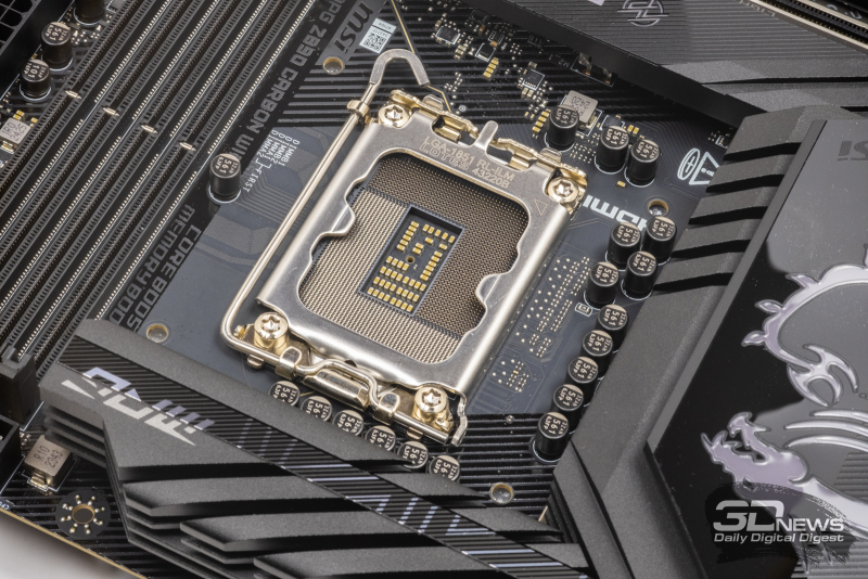
Intel has the usual to change the sockets when this is not really required, but the transition from LGA1700 to the new LGA1851 socket was necessary – it is due to changes in interfaces supported by the processor. In addition to the already familiar PCIe 5.0 X16 for graphics and PCIe 4.0 X4 for SSD, the PCIe 5.0 X4 interface for the most modern and speed drives has been added in new processors. In addition, since the built -in Thunderbolt 4 controller has appeared in Arrow Lake, two corresponding ports with a bandwidth of up to 40 Gbit/s can now be connected to the processor. All this is precisely required by additional contacts of the processor nest.
At the same time, the LGA1851 socket itself looks almost the same as the LGA1700. The new processors retain the dimensions of 37.5 × 45 mm, like Raptor Lake, so the old coolers are quite suitable for desktop systems based on Arrow Lake – there are no changes even in the location of the mounting holes on the motherboards. However, if Arrow Lake and Raptor Lake are placed side by side, then the increased number of contact pads will be clearly visible – they occupy most of the processor belly.
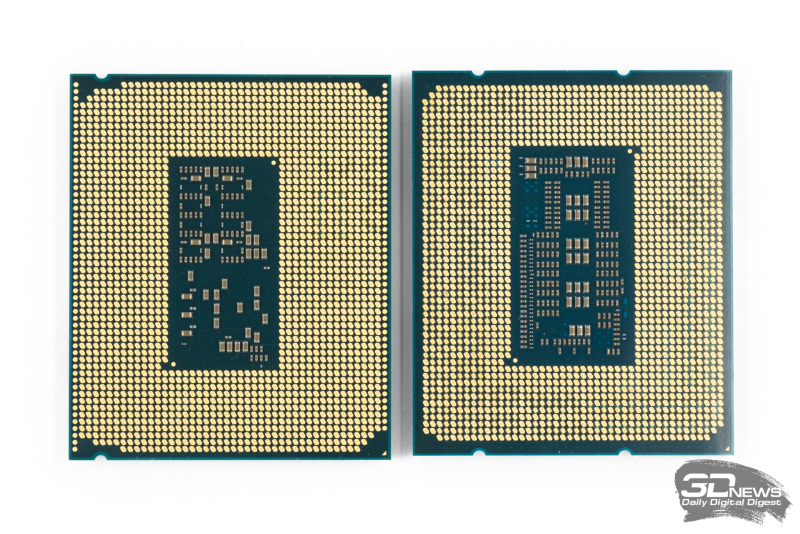
Left – Arrow Lake; right – Raptor Lake
The system logic of the Z890 differs from previous chipsets not too much. The chipset chip, as before, exchange data with the DMI 4.0 X8 tire processor and contains its own PCIE controller with support for 24 lines. However, these lines themselves now work in another speed mode – all of them comply with the PCIe 4.0 standard, and there are no more lines limited by the PCIe 3.0 mode.
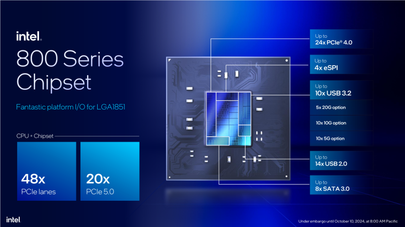
The Z890’s built-in USB controller supports up to 32 USB “lanes” with a bandwidth of 5 Gbps each. They can be combined into different sets, resulting in either simple USB 3.2 Gen 1 (5 Gbps), high-speed USB 3.2 Gen 2 (10 Gbps) or even USB 3.2 Gen 2×2 (20 Gbps) ports. There can be up to 10 ports of the first and second types in systems based on the Z890, and up to five of the fastest USB 3.2 Gen 2×2. In addition, the Z890 still supports 14 slow USB 2.0 ports and 8 SATA ports.
It is quite curious that, having retained some old interfaces, Intel decided to get rid of others. The HD audio interface, codenamed Azalia, went under the knife in the Z890. This means that motherboard manufacturers will no longer be able to use codecs like ALC892 and ALC1200 and will increasingly switch to more modern solutions with USB or I2S/I2C connections.
At the same time, the support of the gigabit network and Wi-Fi 6 remained in the Z890, but Intel does not recommend using these built-in capabilities. According to the company, in the LGA1851 payments you should install faster external network controllers at a speed of at least 2.5 Gb/s along the wire and with support for the wireless standard Wi-Fi 7.
As for the more affordable chipsets, traditionally, in comparison with the Z870, they offer significantly truncated capabilities. The popular B860 limits CPU overclocking and allows only one SSD to be connected to the processor. In addition, the number of supported PCIe 4.0 lanes is limited to 14, and the total number of USB 3.2 ports (any variant) is limited to six.
The budget H610 is even faster. It will not allow you to overclock not only the processor, but also the memory. Boards on it will remain without M.2 slots connected to the processor and will be able to receive no more than two DIMM slots. The maximum number of supported PCIe 4.0 lanes has been reduced to eight, and the number of USB 3.2 ports has been reduced to four.
⇡#New flagship: Core Ultra 9 285k
Before moving on to the results of extensive tests, let’s take a closer look at their main character – the Core Ultra 9 285K.
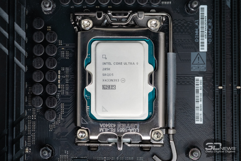
This is the flagship representative in the Arrow Lake desktop family, which has become the ideological successor of the Core i9-14900K. Its new name should not be confusing: if Intel had not decided to redraw the entire naming system for its processors, the Core Ultra 9 285K would probably have been called Core i9-15900K and nothing else. That is, this is a completely familiar processor for desktops, focused on games and everyday work such as creating or editing digital content.
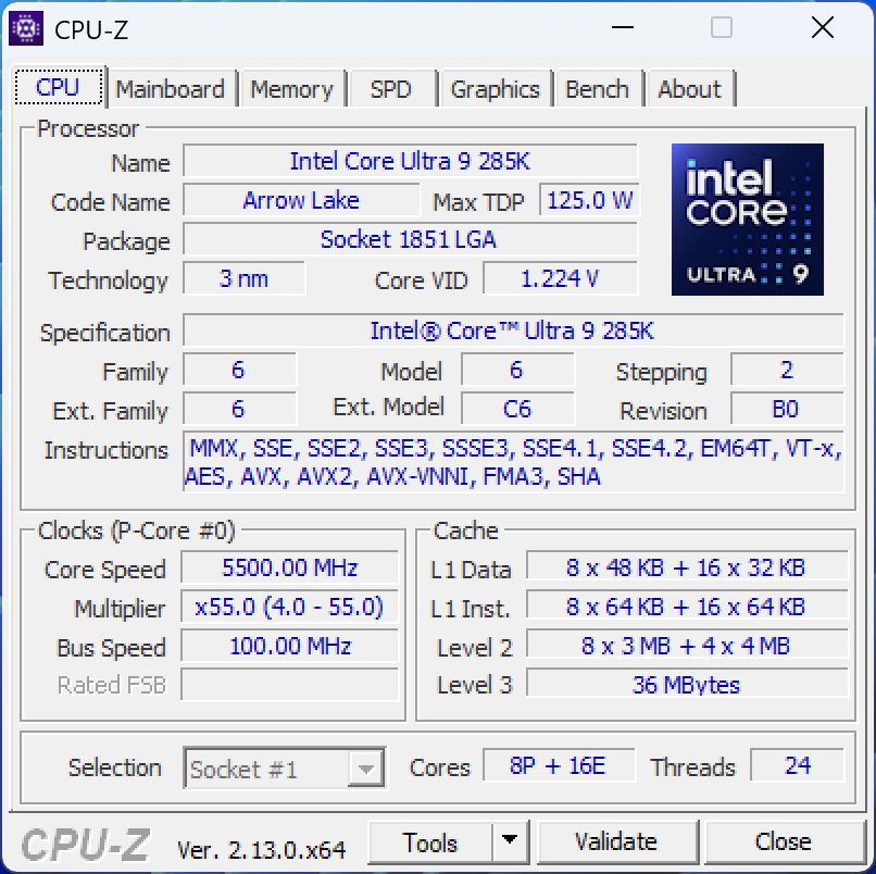
The key specifications of the Core Ultra 9 285K have already been given above: 8 productive and 16 energy-efficient cores, the maximum frequency of the first is 5.7 GHz, the second is 4.6 GHz. These numbers in themselves are not so interesting, but if they are compared with the characteristics of the Core i9-14900K, a rather interesting picture emerges.
The new flagship has lost the frequency of P-cores, but surpasses its predecessor in the frequency of E-cores, which claim to play a much more important role in the new processor. At the same time, due to the lack of Hyper-Threading support, the new Core Ultra 9 285K is inferior to the flagships of previous generations in the maximum number of executable threads. According to this characteristic, it has rolled back closer to the level of the Core i7-14700K and Ryzen 9 9900X, but do not forget that Arrow Lake uses completely different cores.
In addition, the frequency dependence on the load in Core Ultra 9 285k looks a little different when compared with the Core i9-14900K. Measurements of a real -observed frequency during rendering in Cinebench R23 with a limitation of the number of executable flows allow you to get the following schedule.
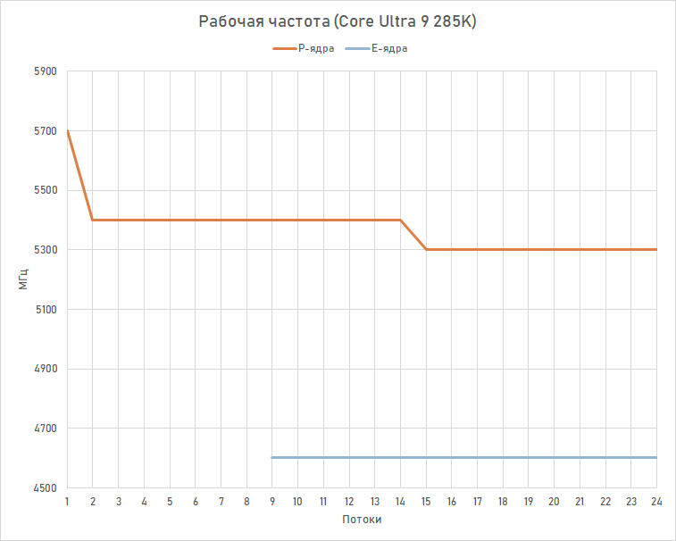
There are no complex dependencies here. The P-cores of the new product almost always operate at a frequency of 5.3-5.4 GHz, and the processor reaches a maximum of 5.7 GHz only in the case of a single-threaded load. At the same time, the E-cores always maintain the maximum 4.6 GHz, regardless of the number of them involved in the work. This means that under intensive multi-threaded workloads, the Core Ultra 9 285K ends up clocking higher than the Core i9-14900K. And this is partly due to the much better energy efficiency of the older Arrow Lake, which, even with a resource-intensive load on all cores, fits into the 250-W budget allocated to it, consuming about 225-230 W.
Another feature of the new product is the large total volume of second-level cache memory. According to this characteristic, it surpasses all x86 CPUs that existed up to this point. However, in terms of total cache size, the Core Ultra 9 285K still loses, and significantly, to competing Ryzen processors with 3D cache.
The official price of the older Arrow Lake is the traditional $589 – the same price received by Intel flagships of previous generations. However, there are two caveats. First, the Core Ultra 9 285K does not have the option with integrated graphics disabled, which existed before and was offered for $25 less. In the current generation of CPUs, -KF modifications remain only in the form of Core Ultra 7 265KF and Core Ultra 5 245KF. Secondly, after the degradation scandal, the price of the Core i9-14900K has dropped significantly, and now it’s impossible to say that the new flagship costs about the same as its predecessor. The actual retail price of the older Raptor Lake is now around $435, so in fact, the Core Ultra 9 285K will cost at least a third more than a processor of the same class from the previous generation.
⇡#Power consumption and temperatures
Intel particularly highlights Arrow Lake’s progress in energy efficiency compared to its predecessors. And according to all preliminary estimates, the new processors should indeed be significantly less power-hungry, both due to the transition to thinner technical processes, and due to architectural changes and disabling Hyper-Threading. And this is easy to see in the test results.
To evaluate the consumption of the Core Ultra 9 285K in a resource-intensive load, we traditionally use the multi-threaded Cinebench 2024 test. And in it, the flagship Arrow Lake really behaves completely differently from its predecessor – it is indeed more economical. While the Core i9-14900K’s consumption hits the 253W limit, the Core Ultra 9 285K doesn’t reach its limit. Its consumption under load on all 24 cores is at the level of 225 W.
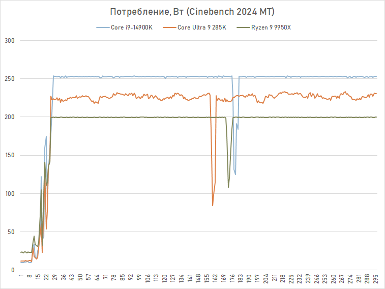
However, this does not particularly affect the temperature regime. Both processors heat up to about 80 degrees. However, in reality, this is a positive sign. AMD experience showed that when switching to thinner processes and reducing the area of crystal with processor nuclei, heat becomes more difficult to remove. But Intel does not have such problems. The Arrow Lake processor crystal, produced according to the 3-nm process, is sufficiently cooled: apparently, it saves that it is more than one and a half times more processor crystal of Zen 4 and Zen 5.
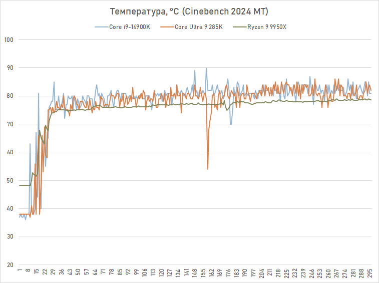
It seemed like a rather frightening symptom that Intel increased the maximum allowed temperature for the Core Ultra 9 285K to 105 degrees. But in fact, this was not done under pressure from circumstances – the new Intel processor does not heat up any more than its predecessors, even under heavy multi-threaded loads.
An even more unexpected picture can be seen when measuring consumption in a single-threaded load in Cinebench 2024. Here, the Core Ultra 9 285K consumes literally half as much as its predecessor, requiring only 35 W of power for rendering with a single P-core. This, naturally, is reflected in the temperature: it is limited to 62 degrees, while the Core i9-14900K is about 10 degrees hotter under the same conditions.
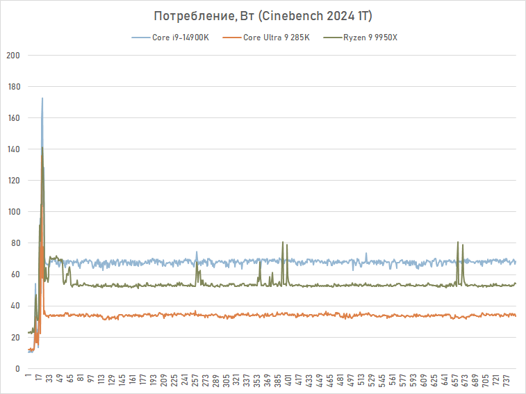
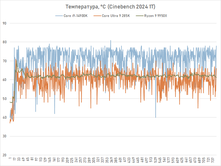
Thus, the Core Ultra 9 285K’s efficiency is better under low-intensity workloads, which is great news for gamers. Games, as a rule, are the type of applications that do not use all the available processor resources, thanks to which Arrow Lake shows its full energy efficiency.
For example, the average consumption of the Core Ultra 9 285K in Cyberpunk 2077 is about 110-120 W, while the Core i9-14900K requires about 160 W of electricity to operate under the same conditions. Of course, this is still noticeably more than the consumption of the Ryzen 7 9800X3D, but the Core Ultra 9 285K is quite comparable to the Ryzen 9 9950X in terms of gaming power consumption.
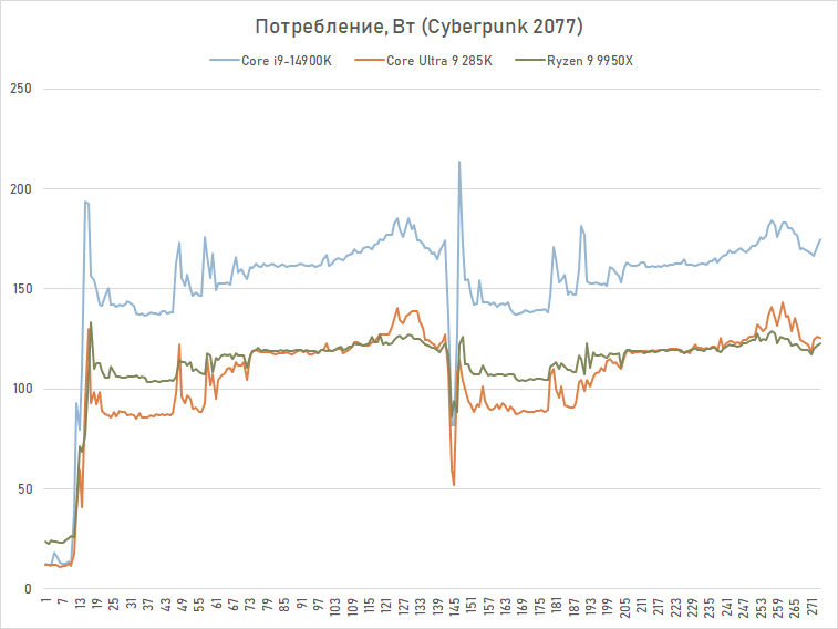
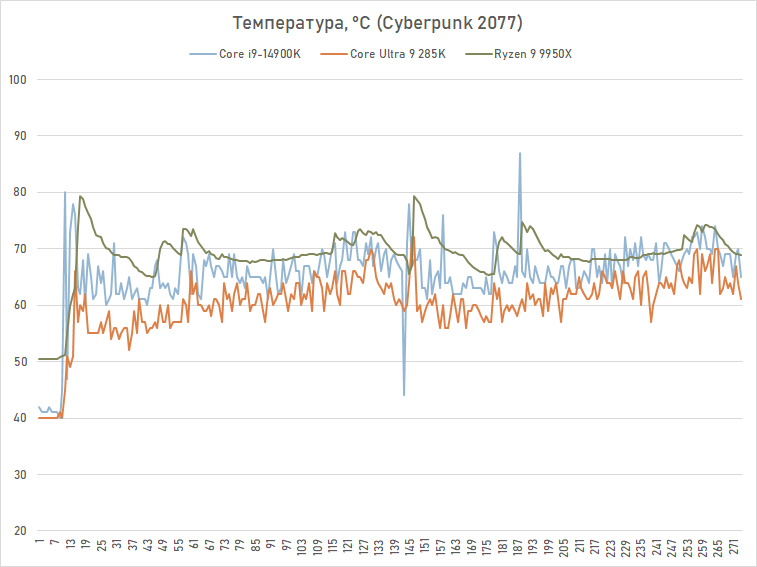
The temperature of the flagship Arrow Lake is noticeably lower than its predecessor. In Cyberpunk 2077, it hovers around 62 degrees, which is even a few degrees lower than the temperature we measured on the Ryzen 7 9800X3D in the same test. As for the Core i9-14900K, it heats up to a temperature of about 68 degrees.
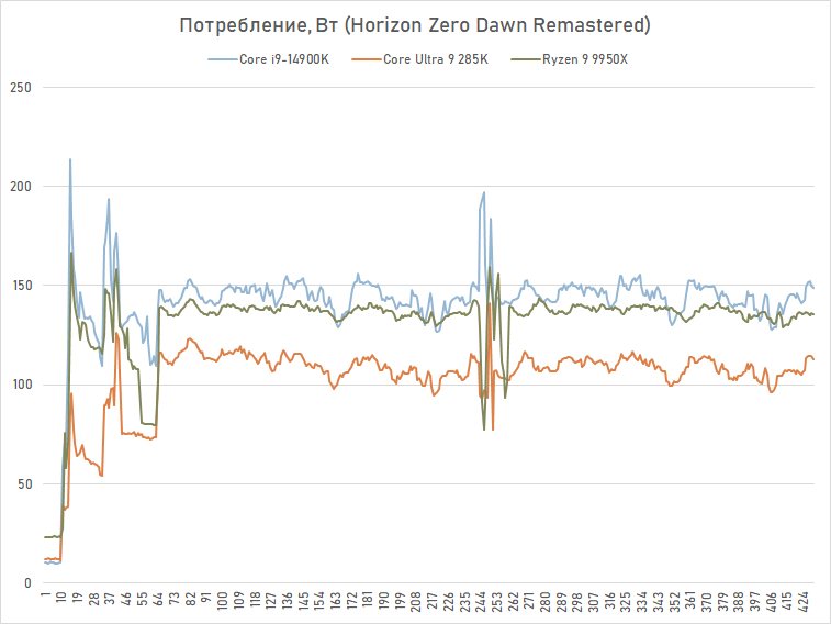
In another game, Horizon Zero Dawn Remastered, the relative energy efficiency of the Core Ultra 9 285K under gaming load is fully confirmed. The average consumption of this processor is 110 W, while the Core i9-14900K at the same time requires about 145 W to operate. For comparison, the consumption of the Ryzen 7 9800X3D in the same game is 95 W, and the Ryzen 9 9950X is 135 W.
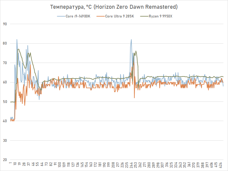
The temperature of the Core Ultra 9 285K is again low, but in this case there is no significant separation in terms of heating from other processors. Temperatures of about 60 degrees in games are typical for modern CPUs, provided that a sufficiently efficient cooling system is used. Only the older Ryzens stand out from this picture, especially the Zen 4 generations, which can heat up much more.
In other words, with the new generation of processors, Intel has really curbed consumption, which has been the subject of serious criticism over the past years. As can be concluded from the test results, on average, the energy appetite of Arrow Lake compared to Raptor Lake decreased by about a quarter. Thus, the flagship Core Ultra 9 285K has become more economical not only compared to the Core i9-13900K and Core i9-14900K, but even compared to the competing Ryzen 9 9950X.
⇡#Description of the test system and testing methodology
Core Ultra 9 285k is the new flagship Intel processor for desktop PCs, so it is logical to compare it with processors of such positioning. However, in addition to the Core i9-14900K and Ryzen 9 9950x, we included two more AMD CPU participants. Firstly, the Ryzen 7 9800x3D, which, albeit not a flagship, but an inaccessible leader in game performance due to the presence of 3D Kesh. And secondly, belonging to the past generation, the 16-core processor Ryzen 9 7950x3D with a 3D-kosh, which still does not have a full-fledged follower in the Ryzen 9000 series.
As a result, the full list of involved components looks like this:
-
- AMD Ryzen 9 9950X (Granite Ridge, 16 cores, 4.3-5.7 GHz, 64 MB L3);
- AMD Ryzen 9 7950X3D (Raphael, 16 cores, 4.2-5.7 GHz, 128 MB L3);
- AMD Ryzen 7 9800X3D (Granite Ridge, 8 cores, 4.7-5.2 GHz, 96 MB L3);
- Intel Core Ultra 9 285K (Arrow Lake, 8P+16E cores, 3.7-5.7/3.2-4.6 GHz, 36 MB L3);
- Intel Core i9-14900K (Raptor Lake Refresh, 8P+16E cores, 3.2-6.0/2.4-4.4 GHz, 36 MB L3).
- CPU cooler: custom liquid cooling system made from EKWB components.
-
- ASUS ROG Maximus Z890 Hero (LGA1851, Intel Z890);
- ASUS ROG Maximus Z790 Apex (LGA1700, Intel Z790);
- MSI MPG X670E Carbon WiFi (Socket AM5, AMD X670E).
- Memory: 2 × 16 GB DDR5-6400 SDRAM (G.Skill Ripjaws S5 F5-6400J3239G16GX2-RS5K).
- Video card: GIGABYTE GeForce RTX 4090 Gaming OC (AD102 2235/2535 MHz, 24 GB GDDR6X 21 Gbps).
- Disk subsystem: Intel SSD 760p 2 TB (SSDPEKKW020T8X1).
- Power supply: ASUS ROG-THOR-1200P (80 Plus Titanium, 1200 W).
Memory subsystems on Intel platforms were configured using the XMP profile of the selected set of modules – DDR5-6400 with timings 32-39-39-102. In the Socket AM5 platform, due to the inability of Ryzen processors with DDR5-6400 to work in synchronous mode, an alternative DDR5-6000 profile with timings of 30-38-38-96 was selected for memory.
Testing took place in the Microsoft Windows 11 Pro (24H2) Build 26100.2605 operating system, which includes all the necessary updates for the correct operation of schedulers on modern AMD and Intel processors. To further improve performance, we disabled “Virtualization Based Security” in Windows Settings and enabled “Hardware Accelerated GPU Scheduling.” The system used the latest graphics driver GeForce 566.36 Driver.
It is also necessary to point out that the BIOS in the Core i9-14900K platform has been updated to a version with Intel microcode 0x12B, which finally eliminates processor degradation associated with the supply of excessive voltages. And the BIOS in the Core Ultra 9 285K platform has been updated to version with Intel microcode 0x114, which should increase the gaming performance of processors from the Arrow Lake family. In addition, both platforms used the Intel Default settings profile, which overrides the “optimizations” introduced by motherboard manufacturers on their own initiative.
Description of tools used to measure computing performance:
Synthetic benchmarks:
- 3DMark Professional Edition 2.29.8256 – testing in the CPU Profile 1.1 scenario in single-threaded and multi-threaded modes.
- Cinebench 2024 – measures single-threaded and multi-threaded CPU performance when rendering in Cinema 4D using the Redshift engine.
- Geekbench 6.3.0 measures single-threaded and multi-threaded CPU performance in common user scenarios, from reading email to image processing.
Tests in applications:
- 7-zip 24.08 – testing compression and decompression speed. A built-in benchmark with a dictionary size of up to 64 MB is used.
- Adobe Photoshop 2024 11.25.0 – testing performance when processing graphic images. The PugetBench for Photoshop 1.0.1 test script is used, simulating basic operations and working with the Camera Raw Filter, Lens Correction, Reduce Noise, Smart Sharpen, Field Blur, Tilt-Shift Blur, Iris Blur, Adaptive Wide Angle, Liquify filters.
- Adobe Photoshop Lightroom Classic 13.4 – testing performance when batch processing a series of images in RAW format. The PugetBench for Lightroom Classic V0.96 test script is used, simulating basic work with the library and editing, as well as import/export, Smart Preview, creating panoramas and HDR images.
- Adobe Premiere Pro 2024 24.5.0 – testing video editing performance. The PugetBench for Premiere Pro 1.1.0 test script is used, which simulates editing 4K videos in different formats, applying various effects to them, and the final rendering for YouTube.
- Blender 4.2.0 – testing the speed of final rendering on the CPU. The standard Blender Benchmark is used.
- Corona 10 — testing the speed of final rendering on CPU. The standard Corona Benchmark is used.
- DaVinci Resolve Studio 19.0 – assessment of video processing performance when encoding with various codecs, processing source files and applying effects. The PugetBench for DaVinci Resolve 1.0 test script is used.
- FastSD CPU-measurement of the speed of quick II generation of images in Stable Diffusion 1.5 in LCM-Lora mode to CPU. The image is created by a resolution of 1024 × 1024 in five iterations.
- Microsoft Visual Studio 2022 (17.13.3)-measuring the compilation time of a large MSVC project —blender version 4.2.0.
- Stockfish 17.0 – testing the speed of the popular chess engine. A standard benchmark with an analysis depth of 28 half-moves is used.
- SVT-AV1 2.1.0 – testing the speed of video transcoding into AV1 format. The original 4K@24FPS video is used with 10-bit color and a bitrate of 51 Mbps.
- Topaz Video AI v5.3.0 – testing performance when improving video quality using AI algorithms executed on the CPU. The original 640×360@30FPS video is upscaled using the Proteus model to a resolution of 1280×720, and the FPS rises to 60 using the Chronos Fast model.
- X264 164 r3186 – testing the speed of video transcoding into H.264/AVC format. The original 4K@24FPS video is used with 10-bit color and a bitrate of 51 Mbps.
- X265 3.6 – testing the speed of video transcoding into H.265/HEVC format. The original 4K@24FPS video is used with 10-bit color and a bitrate of 51 Mbps.
- V-Ray 6.00.01 – testing the speed of final rendering on the CPU. The standard V-Ray 5 Benchmark is used.
Games:
- Assassin’s Creed Mirage. Graphics settings: Graphics Quality = Very High.
- Baldur’s Gate 3. Graphics settings: Vulcan, Overall Preset = Ultra.
- Cities: Skylines II. Настройки графики: Global Graphics Quality = High, Anti-aliasing Quality = Low SMAA, Volumetrics Quality Settings = Disabled, Depth of Field Quality = Disabled, Level of Detail = Low.
- Cyberpunk 2077 2.01. Graphics settings: Quick Preset = RayTracing: Medium.
- Dying Light 2 Stay Human. Graphics settings: Quality = High Quality Raytracing.
- Hitman 3. Настройки графики: Super Sampling = 1.0, Level of Detail = Ultra, Texture Quality = High, Texture Filter = Anisotropic 16x, SSAO = Ultra, Shadow Quality = Ultra, Mirrors Reflection Quality = High, SSR Quality = High, Variable Rate Shading = Quality.
- Hogwarts Legacy. Настройки графики: Global Quality Preset = Ultra, Ray Tracing Quality = Low, Anti-Aliasing Mode = TAA High.
- Horizon Zero Dawn Remastered. Graphics settings: Preset = Very High, Anti-Aliasing = TAA, Upscale Method = Off.
- Marvel’s Spider-Man Remastered. Настройки графики: Preset = Very High, Ray-Traced reflection = On, Reflection Resolution = Very High, Geometry Detail = Very High, Object Range = 10, Anti-Aliasing = TAA.
- Mount & Blade II: Bannerlord. Graphics settings: Overall Preset = Very High.
- Shadow of the Tomb Raider. Настройки графики: DirectX12, Preset = Highest, Anti-Aliasing = TAA, Ray Traced Shadow Quality = Ultra.
- Starfield. Graphics settings: Graphics Preset = Ultra, Upscaling = Off.
- The Riftbreaker. Настройки графики: DirectX12, Texture Quality = High, Raytraced soft shadows = On, Ray traced shadow quality = Ultra, Raytraced ambient occlusion = On.
- The Witcher 3: Wild Hunt 4.04. Graphics settings: Graphics Preset = RT Ultra.
In all game tests, the average number of frames per second, as well as 0.01-quantile (first percentile) for FPS values are given as results. The use of 0.01-quantile instead of the minimum FPS is due to the desire to clear the results from random bursts of performance that were provoked by reasons not directly related to the operation of the main components of the platform.
⇡#Performance in synthetic tests
If we judge the capabilities of the Core Ultra 9 285K solely by synthetic tests, the impression of the new product is very positive. In this study, we used Geekbench 6, 3DMark CPU Profile and Cinebench 2024, and two of the three benchmarks report the superiority of the flagship Arrow Lake over Raptor Lake and Ryzen 9000 in single-threaded performance (this is thanks to the new Lion Cove architecture).


And when assessing multi-threaded performance, all three tests agree that the Core Ultra 9 285K is noticeably faster than both the Core i9-14900K and the Ryzen 9 9950X. The average advantage of the new product over its predecessor is 11%, and over the older representative of the Ryzen 9000 family – 9%.


The problem is that such a preliminary assessment of the performance of the Core Ultra 9 285K using synthetic benchmarks is almost the only section in the entire testing where there is really an opportunity to praise Intel’s new product.
⇡#Performance in demanding applications
Many of the reviews of the Core Ultra 9 285K published by other publications suggest that this processor could be suitable for work systems. However, our in-depth testing shows that such a conclusion is a big stretch. Yes, it is on average faster than the Core i9-14900K in resource-intensive applications. The advantage is about 6%, and in some situations, for example, when working with AI algorithms, it can reach 30-40%. But despite this, Intel has failed to make a processor capable of competing on equal terms in work applications with the Ryzen 9 9950X: AMD’s 16-core product outperforms Intel’s 24-core product in 12 out of 16 tests, ahead by an average of 5%.
At the same time, the Core Ultra 9 285K has obvious weaknesses. Firstly, this processor does not support AVX-512 instructions, which leads to its catastrophic lag behind the Ryzen 9 9950X in applications that actively use them (Topaz Video AI). Secondly, the Core Ultra 9 285K performs poorly where fast work with memory is needed (Photoshop, 7-zip).
In fact, the application performance of the Core Ultra 9 285K is close to the performance of the Ryzen 9 7950X3D, based on the previous Zen 4 architecture. It is likely that if Intel had not disabled Hyper-Threading support in Arrow Lake desktops, the conditional Core Ultra 9 285K would have had a chance to compete with flagship Ryzen generation Zen 5 in applications for creating and processing content, but now its 24 threads are losing 32 threads Ryzen 9 9950X. However, enabling Hyper-Threading would invariably lead to an increase in energy appetite, and now the Core Ultra 9 285K has managed to get closer to the Ryzen 9 9950X in terms of power consumption.
Rendering:


Video transcoding:


Photo processing:


Work with video:


Neural networks:


Compilation:

Archiving:


Chess:

⇡#Gaming performance. 1080p tests
The performance of the Core Ultra 9 285K in games is a rather sad spectacle. The noticeable advantage of the cores of this processor in IPC over its predecessors, the expanded second-level cache and the elimination of Hyper-Threading should have contributed to an increase in gaming performance. But in practice, we see the opposite picture – in terms of average frame rates in games, the Core Ultra 9 285K loses to the Core i9-14900K by about 8%.
And this means that, of course, there can be no talk of any competition with AMD solutions with 3D cache. The average gap between the Core Ultra 9 285K and the Ryzen 7 9800X3D in gaming loads exceeds 15%, which means that the LGA1851 platform cannot be called a gaming platform. Moreover, noticeably better FPS indicators than the Core Ultra 9 285K can be offered not only by the Zen 5 architecture, but even by the previous generation Ryzen 9 7950X3D – its superiority over the older Arrow Lake is 7-8%. In fact, we are talking about the fact that Intel in its new flagship rolled back gaming performance to the level of the Ryzen 9 9950X – a processor that at the time of its release faced sharp criticism, including due to poor performance in modern games.

It’s also worth emphasizing that we conducted this testing after Intel had taken additional measures to improve the performance of the Core Ultra 9 285K. But neither Windows 11 updates nor new microcode versions had any qualitative impact on the situation. The Core Ultra 9 285K remains the worst flagship processor of 2025 for building gaming systems.
And the reasons for this failure lie on the surface. The point, of course, is not the problems with the distribution of threads across cores and errors in the implementation of Thread Director technology, which Intel is struggling with in its patches. The lack of gaming performance is a direct consequence of the high latency of the memory subsystem. Games are one of the most memory-sensitive types of applications, but Intel somehow ignored this point in its Arrow Lake design and allowed latency to increase by almost a third compared to previous CPUs. It would be very naive to expect that a processor with a practical latency when accessing memory of 80-90 ns will be able to show a decent level of FPS.
Moreover, among the games there are those that suffer especially greatly from such an increase in latency. In some of them, the Core Ultra 9 285K loses to the Core i9-14900K in FPS by more than 15% (for example, in Baldur’s Gate 3, Dying Light 2 Stay Human, The Riftbreaker or Hitman 3). And its lag behind the Ryzen 9 9800X3D may even go far beyond the 25% mark.


⇡#Gaming performance. Tests at 2160p
It is generally accepted that in high resolutions the performance of various processors is aligned, and for those gamers who prefer to play 4K, even a processor may be suitable, which showed bad results in the tests in Full HD. This is partly like this: the growth in resolution increases the load on the video card, and the relative contribution of the CPU to the final results becomes definitely lower. Therefore, at first glance, Core Ultra 9 285k seems not so hopeless in this part of the tests.
If we focus on the average FPS for all 14 games used in tests, the older Arrow Lake loses to its predecessor in 4K by only 2.5%, and the Ryzen 7 9800X3D by 4%. But there is a nuance: the situation is very heterogeneous. Among the games there will always be more processor-dependent ones, and in them the Core Ultra 9 285K will be much weaker than the alternatives. For example, in Hitman 3 it is inferior to the Ryzen 7 9800X3D by more than 10%, and in Baldur’s Gate 3 by more than 30%. Therefore, we do not recommend using the Core Ultra 9 285K in any gaming configurations, including those focused on 4K gaming: your favorite game can easily turn out to be processor-dependent.
In addition, even in high resolution, the Core Ultra 9 285K is noticeably inferior to the Ryzen 7 9800X3D not in average, but in minimum FPS, which indicates the worst smoothness of frame changes in configurations based on it. According to this metric, the advantage of the AMD variant is already 6% on average, and in more than a quarter of the games from the test set it exceeds the 10% mark.


⇡#Can Arrow Lake be fixed with fast memory?
Before summing up the final result of acquaintance with Core Ultra 9 285k, I would like to clarify another question regarding his memory controller. Namely, whether it is possible to somehow correct the situation with catastrophically high latency, using the ability of Arrow Lake to work with high-speed memory modules. Intel recommendation to use DDR5-8000 modules with new processors to improve performance did not occur from scratch. Arrow Lake is really able to work stably with an ordinary non-boferized DDR5 memory at a frequency of about 8 GHz, even on boards with four DIMM slots. However, is Core Ultra 9 285K capable of low speed in games?
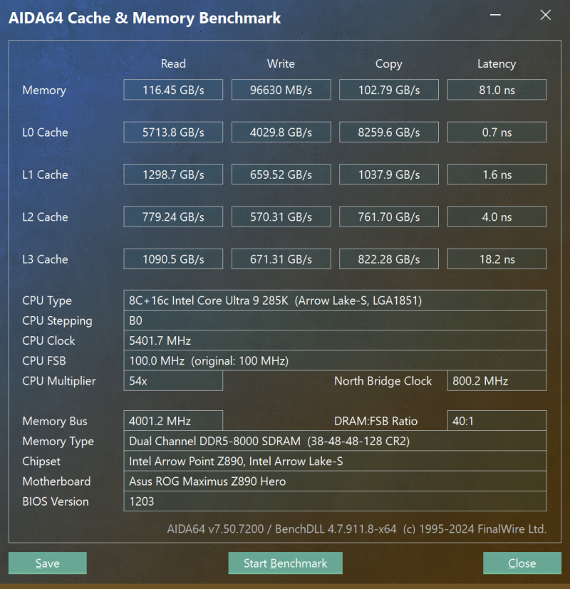
For practical testing, we used a 32 GB set of G.Skill Trident Z5 DDR5-7600 CL36 SDRAM modules. On the LGA1851 platform, this kit is easily overclocked to the DDR5-8000 38-48-48-128 configuration, in which the practical performance of the memory subsystem really becomes higher. It is easy to verify this from the given screenshot of Aida64 Cache & Memory Benchmark.
Core Ultra 9 285K, DDR5-8000


Core Ultra 9 285K, DDR5-6400
Increasing the memory frequency by a quarter led to an increase in read speed by 18%, write speed by 10%, and data copy speed by 11%. It would seem that this is a pretty good effect from overclocking DDR5, but the situation with latency spoils everything. No amount of overclocking of DDR5 modules can eliminate the asynchrony of the line from the processor to the memory, as a result of which the delay when switching to DDR5-8000 is reduced compared to DDR5-6400 by only 6%. Memory latency remains at the level of “above 80 ns”, which means that, frankly speaking, there is nowhere to expect a fundamental improvement in gaming performance.
Testing only confirms this assumption. The average FPS provided in a system with Core Ultra 9 285K when moving from DDR5-6400 to DDR5-8000 increases on average by only 2-3%. This, firstly, indicates a rather weak responsiveness of Arrow Lake performance to memory acceleration, since in the case of Raptor Lake, a similar increase in memory frequency would give at least twice the increase in FPS. Secondly, such an increase is absolutely not enough to change anything. The Core i9-14900K with DDR5-6400 remains a 6% faster gaming combo compared to the Core Ultra 9 285K with DDR5-8000, and the continued overwhelming advantage of the Ryzen 7 9800X3D is not even worth mentioning.
32-39-39-102DDR5-8000,
In other words, the scheme implemented in Arrow Lake, where the memory controller and processor cores are located in different crystals connected by an FDI bus that is not synchronized with either the CPU ring bus or the memory controller, is fundamentally unsuccessful. It seems almost impossible to fix anything here without a hardware redesign, and Arrow Lake’s outstanding DDR5 overclocking capabilities mean next to nothing. Even in games that typically respond very responsively to increased memory speed, the performance of the Arrow Lake platform scales quite modestly. It all comes down to unavoidably high latencies tied to the processor design.
Of course, some kind of change in performance with increasing DDR5 speed is still observed, but the proposed Intel as the “best option” DDR5-8000 does not change the situation with qualitatively, leaving the Core Ultra 9 285k among gaming outsiders. Perhaps a more competitive gaming performance from Core Ultra 9 285k can be obtained with even more speed modules, but to check it, you will have to wait for the appearance of Cudimm modules in the wide sale, the most advanced of which is supposed to be able to move the memory frequency to mark 10 GHC.
⇡#Conclusions
Core Ultra 9 285K is a very controversial new product. On the one hand, Intel has taken several positive steps, thanks to which Arrow Lake has risen significantly above Raptor Lake on the evolutionary ladder. The updated core architecture led to an increase in IPC. The processor received a new multi-chip structure, which made it possible to optimize production and cost. The most important components have moved to an advanced 3 nm process technology, making Arrow Lake noticeably more energy efficient compared to its predecessors. In addition, the platform has been upgraded: the number of supported PCIe 5.0 lanes has increased and the ability to support high-speed memory has improved.
However, all these advantages fade against the background of real results of Core Ultra 9 285k in performance tests. Here he literally fails with a bang: the increase in difficult tasks compared to Core i9-14900K is not serious 6 %, and the games noted the average FPS by 8 %.
The cause of the disaster is quite obvious. Firstly, Intel deliberately limited the performance of P-cores by lowering their frequency and disabling support for Hyper-Threading, which negatively affected multi-threaded work. Secondly, the transition to a multi-chip layout led to a slowdown of the memory controller. Its latency increased by 20–25 ns, and this greatly affected the speed of memory-sensitive applications, primarily gaming ones.
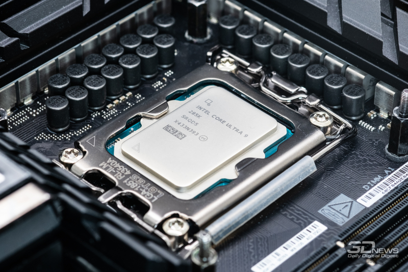
As a result, the Core Ultra 9 285K is unlikely to become a popular processor, because when building a modern PC for any purpose, you can choose an alternative from AMD with a clearly more favorable price-performance ratio. Thus, the Ryzen 7 9800X3D offers significantly better performance in the gaming segment, and in professional tasks the Ryzen 9 9950X is a more productive solution. Moreover, the upcoming version of the 16-core AMD with 3D cache will certainly provide an even greater lead. In other words, even taking into account the improved energy efficiency, competition with modern AMD products remains beyond the capabilities of the Core Ultra 9 285K.
It was assumed that Arrow Lake processors would improve Intel’s market position in the desktop segment after the Raptor Lake degradation scandal and would become a response to the AMD Ryzen 9000 family. However, it turned out that their appearance only made Intel’s position worse. It comes to the point that in current conditions, the more logical option for Intel supporters is to buy chips from previous generations, rather than switching to the new LGA1851 platform with the very controversial Arrow Lake processor family.
And the saddest thing is that the lack of decent Intel solutions for desktop computers will last for a very long time, since the company will not be able to offer next-generation products until the end of 2026. This means that in the coming months, competition in the desktop processor market will steadily weaken, which is unlikely to benefit consumers.