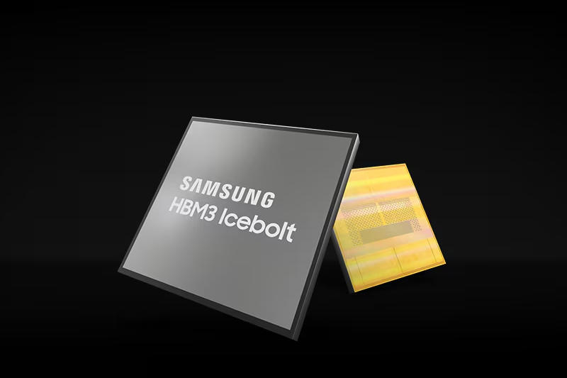
The memory components industry is distinguished by a conservative approach: manufacturers prefer gradual improvements to revolutionary changes. But by the end of the decade, monolithic 3D DRAM may be introduced to the world, although it is not yet clear what form this solution will take and when such memory will be ready for mass production.

Image source: samsung.com
In the field of flash memory, manufacturers have achieved significant success – the capacity of components is increased due to monolithic 3D architecture. But in the field of DRAM, this solution cannot be used, because there is a need for large enough elements to store charge – as a rule, these are capacitors. The simplest approach to increasing the amount of data on a single-layer DRAM chip is to reduce the cell size. Vertical capacitors make the DRAM layers too thick, making it difficult to stack them on top of each other. To solve this problem, some manufacturers try to place capacitors horizontally, while others try to eliminate them altogether.
3D DRAM can have various implementations. One of them is already used in production – high-bandwidth memory (HBM), but in this case we are talking about a multi-layer chip, and not a monolithic one, as in the case of 3D NAND. The advent of monolithic 3D DRAM chip will give impetus to the development of HBM and will have an impact on the entire industry. DRAM cells can be optimized by reducing feature sizes using advanced lithography techniques, such as creating preforms in two or four passes. Samsung is developing a new 4F2 cell architecture, more compact than the current 6F2, but its creation will require new materials, including ferroelectrics.
Another promising direction is to lay the capacitor on its side, which will help reduce the thickness of the layers in order to arrange these layers vertically. Chip manufacturing equipment manufacturer Lam Research has proposed several ways to achieve this goal: inverting the cell, shifting the bit line, and using gate-ambient transistors (GAAs). DRAM designs without capacitors are being considered; Floating Body DRAM (FB-DRAM) technology is proposed, similar to floating-gate flash memory. Neo Semiconductor has proposed a commercial technology based on the double gate Floating Body cell. Simulations showed that “this mechanism can improve sensitivity margin and data retention,” said company CEO Andy Hsu. Thus, the advent of monolithic 3D DRAM may indeed be around the corner, but it will take several more years for manufacturers to allocate funds to support one of the solutions.