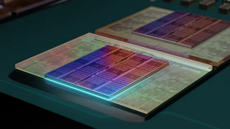
Semiconductor analyst Tom Wassick disassembled the crystal of the best gaming processor of our time, the Ryzen 7 9800X3D, layer by layer, and found out that most of the volume is a dummy.

Image Source: AMD
Unlike the Ryzen 5000X3D and Ryzen 7000X3D, the Ryzen 9000X3D processors are structured so that a layer of additional SRAM memory (3D V-Cache) is located under the heat-generating CCD block with the compute cores, rather than above it. While AMD hasn’t revealed the ins and outs of this approach, this on-chip structure offers better thermal balance and allows the processor to achieve higher clock speeds.
Wassik notes that the CCD block and 3D V-Cache layer are made very thin, less than 10 microns, to ensure TSV soldering. In combination with BEOL (Back-end of Line) – interconnects based on metal layers for connecting individual components of the chip – the total thickness of the SRAM memory layer and the CCD chiplet is 40-45 microns.
The SRAM memory in the Ryzen X3D has always occupied only a fraction of the total die area. For example, the Ryzen 7000X3D chips have a 3D V-Cache layer area of 36 mm2, while the area of the entire CCD block is 66.3 mm2. However, Tom Wassik’s research shows that the SRAM layer within the Ryzen 9000X3D is actually 50 microns larger than its CCD area. This suggests that most of the Ryzen 7 9800X3D die does not contain any functional blocks and is a dummy. However, more detailed research is needed to make accurate conclusions.
Excluding interconnects, the total thickness of the SRAM layer and the CCD chip should be less than 20 microns. To accommodate such small and fragile components, AMD added bulky layers of empty silicon on top and bottom for structural integrity. The thickness of the entire stack is approximately 800 µm. Minus the 50 µm in CCD, SRAM and BEOL, we get a whopping 750 µm of structural support. In other words, up to 93% of the entire die stack can be silicon without transistors.
Between the different layers of the crystal are also layers of oxide coating. The thickness of this bonding layer between the CCD die and the SRAM is thinner than that between the dummy silicon and the two dies, resulting in better thermal performance. Some features of the crystal structure of Ryzen 9000X3D processors have not been fully studied. Tom Wassik plans to study them using a scanning electron microscope in the future.
Although Intel has lost the title of manufacturer of the fastest gaming processors, the company has no plans to release an analogue of 3D V-Cache technology for consumer chips. AMD, meanwhile, is expected to unveil the 12-core Ryzen 9 9900X3D and 16-core Ryzen 9 9950X3D at CES 2025 next month.