Recently, at the IEDM 2024 conference in San Francisco, TSMC for the first time officially spoke about the advantages of moving to 2nm transistors with a Gate-All-Around circular gate and nanosheet channels. The Taiwanese chipmaker will begin producing chips using N2 technology in the coming year. In fact, nanosheets are the final architecture of transistors in the usual sense and it will remain relevant for a long time.

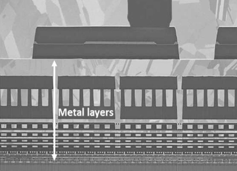
Don’t see the 2nm transistors at the bottom? And they exist! Image Source: TSMC
In 2025, Samsung and Intel will also begin producing chips based on a 2nm process technology with nanopage channels and a circular gate. Samsung was the first to produce such structures within the 3nm process in 2022. For TSMC, this will be the first experience and the fruit of “more than four years of work,” as the head of the company’s development department admitted.
Modern FinFET transistors are a set of vertically located transistor channels – ribs or fins. The characteristics of such a transistor depend on the number of edges each has – one, two or three. The more channels, the larger the area occupied by the transistor. This is especially acute in the case of SRAM memory arrays. Each cell of such memory consists of six transistors and is therefore difficult to scale. Meanwhile, neither simple controllers nor powerful processors and accelerators can do without SRAM.
Translating transistor channels into a horizontal plane in the form of thin nanopages immediately improves density, since the channels are located on top of each other, no matter how many there are. This does not increase the space occupied by the transistor. In particular, TSMC’s move from 3nm FinFET to 2nm nanopage transistors increases transistor density by 15%, regardless of whether it uses high-performance or power-efficient circuits. There will be a win in both cases.
You have to choose between productivity and energy efficiency. If you rely on computational speed, the gain from switching to 2nm nanopage transistors will be 15%, and if you choose low consumption, the gain will reach an impressive 30%. But this is not the whole benefit of nanopage channels. For FinFET transistors, it is impossible to create transistors with 1.5 edges – this is like one and a half diggers from a famous fairy tale. But in the case of nanopage channels, you can change their width, not to mention their number, and design circuits with various and precisely required parameters.
TSMC called the technology for changing the width of nanopages Nanoflex. This will make it possible to produce logic with narrow nanopages on the same chip, which will limit their consumption, and a computing core with transistors with wide nanopages to pass high currents, which will ensure performance no matter what.
But SRAM will especially benefit from the transition to nanopage transistor channels. When moving from 4nm to 3nm process technology, the density of SRAM memory cells increased by only 6%. In the case of Nanoflex technology, when moving from 3-nm to 2-nm process technology, the density of SRAM cells will increase by 11%. This will provide widespread gains, TSMC says.

Image Source: Intel
It is interesting to add that at the same conference there was a report from Intel, which outlined the boundaries of the future for classical transistors and, specifically, in nanopage design.
«Nanopage architecture is really the last frontier of transistor architecture, said Ashish Agrawal, a silicon scientist in Intel’s circuit components research group. “Even future complementary FET (CFET) devices, which may appear in the mid-2030s, will be built from nanosheets. Therefore, it is important that researchers understand their limitations.”
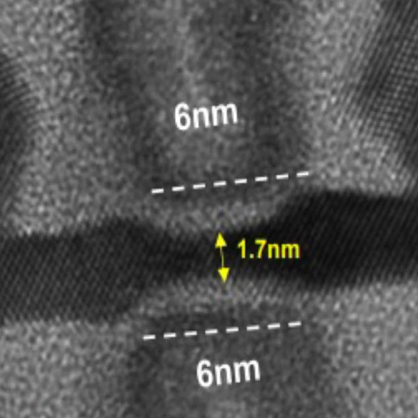
To explore the boundaries of what is possible, Intel created an experimental transistor structure with a 6 nm channel. The shorter the channel, the higher the probability of leakage through it and the less controllable the transistor becomes. The experiment showed that transistors with channels 6 nm long and a nanopage width 2 nm are fully operational. This will allow nanopage transistor architecture to exist for a long time, pushing the transition to two-dimensional materials and transistors on a fundamentally different architecture far into the future.
Returning to TSMC’s (as well as Samsung and Intel’s) 2nm process technology, let us recall that the number in its name says nothing about the physical dimensions of the transistors. Within the 2nm process technology, transistors and transistor channels are measured in tens of nanometers. Therefore, it will take more than five years for the industry to reach the boundaries set by Intel in the experiment.