Today’s advanced computing components typically use advanced chip packaging even when they contain a single monolithic die. The significance of progress in the field of chip packaging is growing due to the transition of most developers to a multi-chip layout. Amkor and TSMC have agreed to collaborate in this area at both companies’ facilities in Arizona.
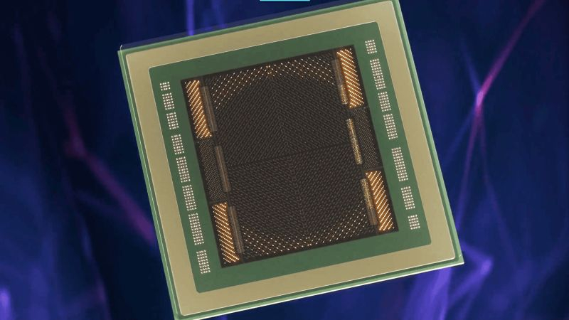
Image source: Amkor
Amkor will help TSMC create all the infrastructure necessary for testing and packaging chips using modern technologies in Arizona, where the latter is building facilities intended for contract manufacturing of chips for American customers. The Amkor facility will be located in the city of Peoria in this state, which will serve TSMC’s interests in testing and packaging chips. Its proximity to TSMC’s silicon wafer processing facilities will reduce chip manufacturing times and eliminate the geopolitical risks associated with these types of Asian facilities.
The parties must, in accordance with the current situation, determine the types of packaging used, but InFO and CoWoS will certainly be included in their list. Amkor is the world’s largest provider of chip testing and packaging services, operating since 1968. The American origin of this partner is intended to provide the reliability of interaction necessary for the success of the TSMC project in Arizona. The irony is that Amkor has historically located its operations outside the United States, and only $600 million in subsidies allowed it to decide to build a large plant in Arizona by 2027.