Power electronics are in demand these days due to the electrification of transport, and a promising direction for its development is the production of gallium nitride (GaN) components that can withstand higher loads and temperatures compared to silicon. Infineon was the first among its competitors to master the technology for producing such components on wafers with a diameter of 300 mm.
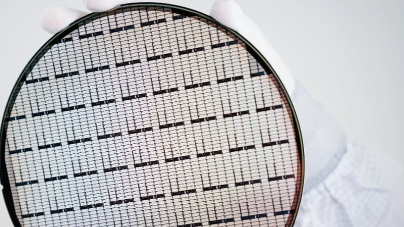
Image source: Infineon Technologies
Until now, gallium nitride components have been produced using 200 mm wafers, so increasing the diameter by one and a half times will help reduce the cost of such products, since 2.3 times more chips can be produced from one wafer, and some fixed costs can be distributed across larger volume of products. According to Infineon representatives, the company’s customers will receive the first samples of products manufactured using this method in the fourth quarter of 2025.
In addition to the automotive industry, gallium nitride chips will find application in the PC segment, consumer electronics, server equipment, robotics and industrial automation. In the same server systems, the use of components of this type will allow the creation of more compact and efficient power supplies. It is important that 300 mm gallium nitride wafers can be processed on existing equipment suitable for working with silicon components. The Austrian company Infineon will be the first to introduce this production technology.
In the future, the cost of GaN components will be equal to that of silicon, as Infineon management is convinced, and the transition to a wafer size of 300 mm will greatly contribute to this. Increasing the diameter of substrates when working with this material is largely complicated by the fact that it is necessary to maintain uniform distribution of the material over the plate. An alternative direction in the development of power electronics is the use of silicon carbide, but in this area the size of the processed wafers has only increased from 150 to 200 mm. Infineon produces such chips at its plant in Malaysia, which is the largest in the world. The market for gallium nitride components is expected to increase ninefold to $2.25 billion by 2029, according to Yole analysts.