NEO Semiconductor has introduced 3D X-AI chips designed to replace HBM memory, which is used in modern GPU-based accelerators. 3D DRAM memory has a built-in AI processing engine that handles data streams without requiring mathematical calculations. This helps solve the bus width problem between the processor and memory, helping improve the performance and efficiency of AI systems.
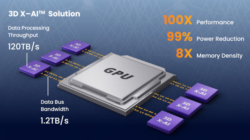
Image source: NEO Semiconductor
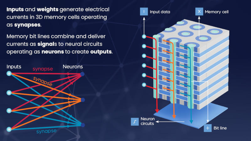
At the heart of the 3D X-AI chip is a layer of neural circuitry that processes data from 300 layers of memory on the same chip. The memory density on the component is eight times higher than that of the current HBM, and 8000 neural circuits provide a 100-fold increase in performance due to data processing directly in memory – the volume of data is radically reduced, which reduces the accelerator’s energy consumption by 99%.
«Existing AI chips waste significant performance and power resources due to architectural and technological inefficiencies. Today’s AI chip architecture stores data in the HBM and delegates all computation to the GPU. This architecture of separated data storage and processing inevitably turns the bus into a performance bottleneck. Transferring huge amounts of data through the bus reduces performance and greatly increases energy consumption. 3D X-AI can perform AI processing in each HBM chip. This can significantly reduce the amount of data transferred between the HBM and the GPU to improve performance and significantly reduce power consumption,” said NEO Semiconductor founder and CEO Andy Hsu.
A single 3D X-AI die has a capacity of 128 GB and offers AI processing speeds of 10 TB/s. Twelve dies in one HBM package can provide 1.5 TB of memory with a bandwidth of 120 TB/s. Developers of AI processing hardware are exploring solutions that can improve their throughput and speed – semiconductors are becoming faster and more efficient, but the bus between components is often a bottleneck. Intel, Kioxia and TSMC, for example, are working on optical technologies to speed up communication between components on a motherboard. By moving some of the AI workload processing from the GPU to the HBM, NEO Semiconductor’s solution can make accelerators much more efficient than they are today.