The shortage of CoWoS chip packaging capacity is forcing TSMC to rapidly increase it; it plans to double its productivity in this area this year, and has already begun equipping its largest plant in this profile, AP8, which it bought from display manufacturer Innolux last year.
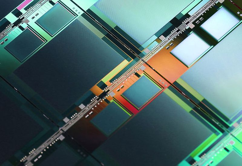
Image Source: TSMC
The specifics of LCD panel production and chip packaging overlap in some ways, which is why TSMC was able to quickly and cost-effectively retool the Innolux facility to suit its needs. The factory in southern Taiwan has clean rooms with a total area of 100,000 m², and by this criterion is the largest on TSMC’s balance sheet. For example, the existing AP5 facility is four times smaller than the new one. Accordingly, after AP8 is put into operation in the next few months, TSMC will significantly increase its capacity for chip packaging using the CoWoS method. It is expected that AP8 will start operating in six months, thereby significantly contributing to the reduction of the shortage of Nvidia chips for computing accelerators, which are manufactured using the CoWoS method.
TSMC specialists have gained extensive experience in installing and configuring the relevant equipment, so the time spent on its launch at a specific production site can be reduced compared to the typical six months. According to experts, the rate of expansion of capacities for packaging chips using the CoWoS method will increase to 124.3% this year compared to 105.6% last year, but next year it will decrease to 34.9%. This will be affected not only by market saturation, but also by the migration to other chip packaging methods that has begun. In addition to SoIC and CoPoS, TSMC will offer SoW and WMCM to customers.