Samsung expects to have its first High-NA EUV lithography system by the end of this year

The South Korean company Samsung Electronics not only remains the largest memory manufacturer, but also does not abandon its ambitions in the field of contract manufacturing of logic components. In order to keep pace with progress, it is going to follow Intel by the end of this year to receive the ASML TwinScan EXE:5000 lithography scanner, which allows working with a high numerical aperture (High-NA).

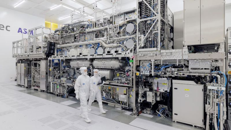
Image Source: ASML
Intel is ASML’s largest customer in this area and is trying to buy out all similar systems available for order this year, but Samsung’s intentions show that with some persistence, the Korean company can also receive its first High-NA EUV lithography system by the end of this year or in first quarter of next. Such equipment should allow Samsung not only to start producing chips using technologies “thinner” than 2 nm, but also to do this at a lower cost. True, a lithographic scanner of this class costs at least $380 million, and it also takes up more space, so the implementation of such equipment will require not only high initial costs, but also a change in the approach to workshop layout.
Along the way, South Korean media report that Samsung admitted that it has inspection tools for photo masks of the Japanese brand Lasertec, which are adapted to High-NA EUV technology. If everything goes according to plan, Samsung will be able to start producing the first prototypes of products using equipment of this class by the middle of next year. However, the company will master the High-NA EUV technology in mass production closer to 2027.
Samsung, in collaboration with Synopsys, is also introducing a different “pattern” of semiconductor chip elements, which involves a transition from straight lines to curves. This will make it possible to create denser structures on chips and advance the development of more “fine” technical processes. TSMC also expects to receive its first High-NA EUV lithography scanner from ASML by the end of the year, but plans to introduce such equipment in the mass production of chips using A14 technology no earlier than 2028.

Recent Posts
A demo of Dispatch, a comedy game about a superhero agency from the former developers of Tales from the Borderlands and The Wolf Among Us, has been released on Steam
Developers from the American AdHoc Studio, founded by former Telltale Games, Ubisoft and Night School…
Digma DP-FHD800A LCD Full HD Projector Review: A Modern Approach
When you think about a home theater, you immediately imagine bulky projectors with a bunch…
Lian Li Introduces HydroShift II LCD-C Liquid Cooling System with 360mm Radiator and Three Configurations
Lian Li has introduced a series of maintenance-free liquid cooling systems HydroShift II LCD-C. It…
Apple: App Store App Developers to Earn $406 Billion in 2024
Amid mounting pressure from U.S. regulators, Apple has released the results of an independent study…
ASRock Admits Its Motherboards Break Ryzen 9000 Processors
Following a report from YouTube channel Tech Yes City that ASRock linked Ryzen 9000 processor…
Apple to Change OS Numbering: iOS 26 to Come This Year Instead of iOS 19
Apple is preparing a large-scale rebranding of its line of operating systems. This was reported…