The situation around the technological difficulties that Samsung Electronics is facing is surrounded by a considerable number of rumors and speculations. Some sources stated the day before that Samsung had despaired of advancing in mastering new lithographic standards and would refuse to switch to the 1.4-nm process technology. The company later denied these rumors.
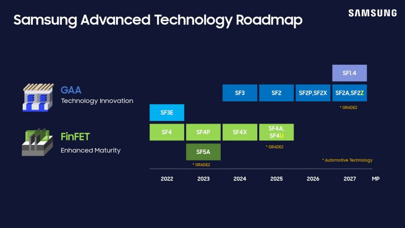
Image source: ComputerBase.de
As ComputerBase notes with reference to the South Korean press, the refutation of rumors about Samsung’s refusal to master 1.4-nm technology was announced at the general meeting of the company’s shareholders. According to Samsung management, following the 2-nm family of technological processes, 1-nm class technological processes will be mastered. At the same time, the timing of their implementation was not named, but if we focus on the existing slides from Samsung presentations, this will happen no earlier than 2027. The possibility of some delay cannot be ruled out, because this area of activity is fraught with many unpleasant surprises and risks.
Nvidia CEO Jensen Huang, who traditionally stirs up interest in the topic of his company’s cooperation with Samsung in the field of purchasing memory for AI accelerators, expressed hope this week that the HBM3E chips produced by this Korean company can be used in the release of accelerators of the Blackwell Ultra family, nominally presented the day before. The GB300 accelerator, for example, will rely on up to 288 GB of HBM3E memory, which will be distributed across eight 12-tier stacks. The debut of Blackwell Ultra is scheduled for the second half of the year, so Samsung formally has enough time to rehabilitate itself in the eyes of investors and its main partner in this area, Nvidia.