In an effort to distract from rumors that it is seeking a strategic partner in chip manufacturing, Intel executives this week said that they have successfully used the latest generation of lithography systems from ASML to manufacture chips in small batches. Using High-NA EUV technology, the company was able to process 30,000 silicon wafers in a single quarter.
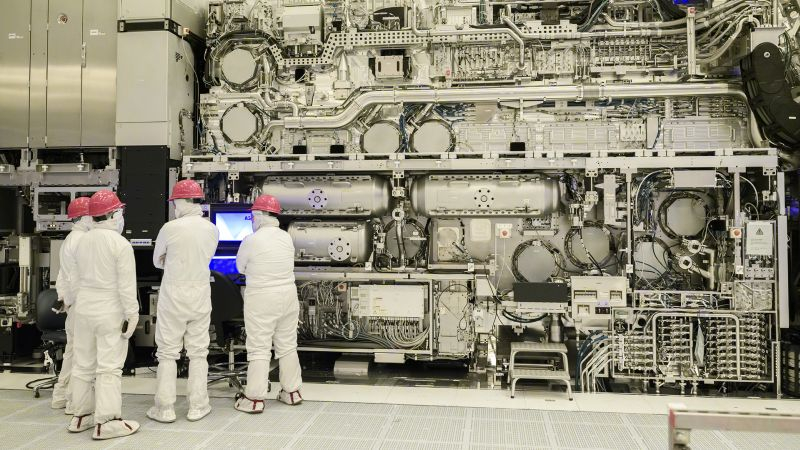
Image Source: Intel
Intel received ASML’s High-NA EUV lithography equipment last year, and two systems (presumably TwinScan EXE:5000) are already set up to produce pilot products in sufficient quantities. According to Intel representatives, the new equipment allows for a reduction in the number of process steps in the production of modern chips and an acceleration in the manufacture of advanced products. Intel spent a total of seven years preparing to launch this technology.
Early experiments had reliability issues with EUV systems, but High-NA EUV equipment is twice as reliable as previous-generation solutions, according to Intel lead engineer Steve Carson. The manufacturing cycle time is reduced by switching to high numerical aperture equipment. For example, if previously three exposures and 40 process operations were required to process a silicon wafer, now the number of the latter has been reduced to less than ten, and only one exposure is required.
As is known, Intel used High-NA EUV equipment as an experimental one in preparation for the release of chips based on Intel 18A technology, but it will not be used in the serial version. It should be implemented already during the release of chips based on Intel 14A technology no earlier than next year. At the same time, even newer ASML equipment of the TwinScan EXE:5200 family will be used, the first components of which the company should receive in the coming months. Competing TSMC will make the transition to High-NA EUV no earlier than 2028, as experts expect.