Late last month, Intel officially announced its readiness to provide finished digital designs of products by the end of this half-year, which it plans to manufacture for customers using the advanced 18A technology. Later, Intel representatives denied rumors about a delay in mastering this technological process, and now it has become known that it has begun to be used at the company’s enterprises in Arizona.
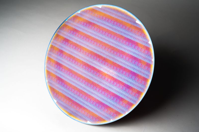
Image Source: Intel
As TechPowerUp notes, Intel engineering project manager Pankaj Marria reported on his LinkedIn page that test silicon wafers with components processed using the 18A technology have been successfully manufactured at a facility in Arizona. The geographic location is important because Intel initially implemented this technology on production lines located in close proximity to its research center in Oregon. In the future, the use of the 18A process technology is planned for Intel’s Arizona facilities, so the new revelations from the company’s specialists allow us to talk about the success of this expansion.
The corresponding stage of Intel 18A implementation even has a symbolic banner with the words “the eagle has landed”. The company expects to start mass production of products using Intel 18A technology in the second half of this year, but even from the words of Intel management it is clear that its own products of this generation will begin to enter the market in mass quantities no earlier than next year. Most likely, products for third-party customers manufactured using Intel 18A technology will appear a little later. The 18A process technology was supposed to be implemented at Intel’s plants under construction in Ohio, but they are delayed until 2030, when it will already be in less demand, and the company’s plans in this area have probably changed significantly.