In Japan, the EUV scanner has been significantly simplified, which can dramatically reduce the cost of producing advanced chips

Professor Tsumoru Shintake of the Okinawa Institute of Science and Technology (OIST) has developed a significantly simplified EUV lithography tool that is significantly cheaper than ASML scanners. The lithographic system he proposed uses two mirrors instead of six. If the device goes into mass production, it could transform the chip manufacturing equipment industry, if not the entire semiconductor industry.

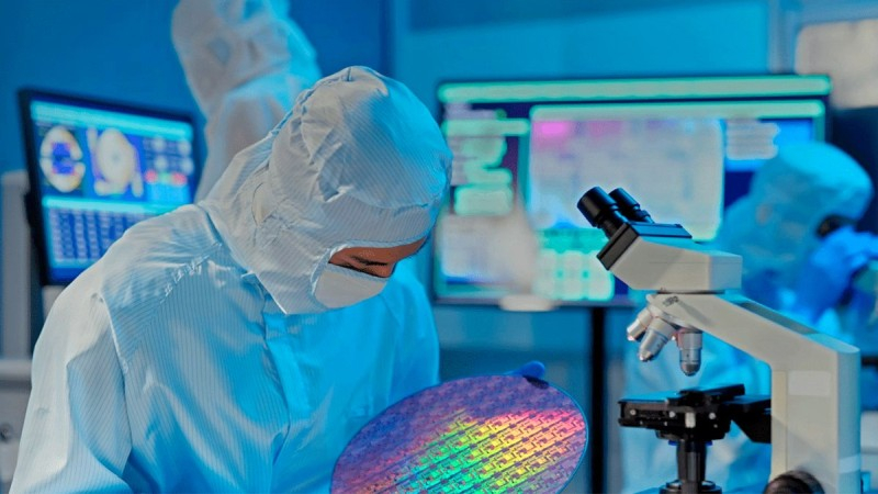
Image source: Samsung
The new system uses only two mirrors in its optical projection setup, which is a significant departure from the traditional six-mirror configuration. The new shorter optical path allows more than 10% of the initial EUV energy to reach the wafer, compared to about 1% in currently used installations, which is a major breakthrough.
Professor Shintake’s team has addressed two major challenges in EUV lithography: preventing optical aberrations and ensuring efficient light transmission. The “dual linear field” method they developed exposes the photomask, minimizing distortion and increasing image fidelity on the silicon wafer.

Image source: OIST
One of the key advantages of the proposed solution is increased reliability and ease of equipment maintenance. An equally significant advantage of this design was the radical reduction in energy consumption. Thanks to the optimized optical path, the system uses an EUV light source of only 20 W, and the total power consumption is less than 100 kW, which is an order of magnitude lower than the requirement of traditional EUV lithography systems. Thanks to reduced energy consumption, the cooling system is also simplified and cheaper.
The performance of the new system was extensively tested using optical simulation software, confirming its ability to produce advanced semiconductors. Scientists have filed a patent application, indicating that the new technology is ready for commercial implementation. The developers view the new EUV lithography system as an important step towards reducing power consumption and other costs of chip production, but specific dates for the start of commercial operation of the new scanner have not yet been announced.
The economic implications of the invention are very promising. The global EUV lithography market is expected to grow from $8.9 billion in 2024 to $17.4 billion by 2030.

Recent Posts
FTC’s ‘One-Click Unsubscribe’ Rule Delayed Again, But Not for Long
The US Federal Trade Commission (FTC) has delayed a rule that would require companies to…
KIBORG: left – crown, right – augmented. Review
Played on PC Developers from Sobaka Studio have built a reputation for themselves as authors…
A simple and reliable speedometer for satellites has been invented in the USA
Satellites move in orbit at speeds of thousands of kilometers per hour, and without precise…
Schoolchildren are starting to stick metal objects into Chromebook ports en masse for TikTok likes
A dangerous new TikTok challenge has gone viral in which American schoolchildren are deliberately damaging…
Apple is developing powerful Baltra processors for AI servers, as well as consumer M5, M6 and M7
Apple is developing processors for data centers that will serve requests from Apple Intelligence artificial…
Despelote — goo-o-o-o-o-o-o-o-o-o-ol! Review
One of my first memories (or perhaps the very first one – is it possible…