IBM has extended optical fiber to the processor – this will speed up the training of artificial intelligence by 80 times

Over the past twenty years, computing and communications have been moving to optical interfaces. This has already happened on the backbone communication lines, but is still stalled within data centers and at the level of interchip and intercomponent communications in computers. Ideally, the signal should immediately come from the processor in the form of optical pulses and then be sent either to the chip next door, or to neighboring racks, the hall, and even beyond. IBM chose this path.

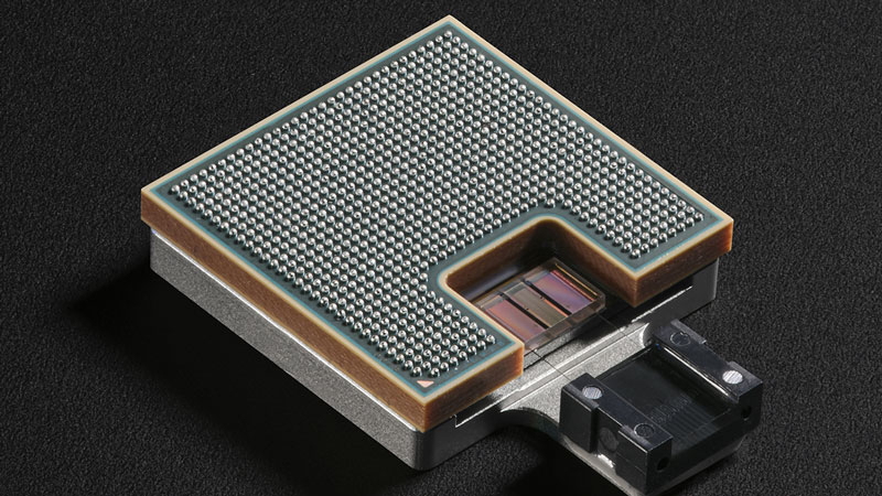
CPO slot for installing an external optical “cable” on the chip. Image source: IBM
Optics compares favorably with copper (conductive connections) in its light weight, low cost, low interference (noise), high transmission speed, low energy consumption and, in general, allows you to increase throughput without increasing energy consumption. The ability to use optical communication lines is already included in all the latest Ethernet standards, as well as PCIe standards. Intel came closest to integrating optical lines into processors (accelerators) with its Light Peak platform. And although Intel stopped developing this platform a long time ago, the idea has not died and today is continued in the new optical interface Intel OCI (Open Compute Project Interconnect Link).
Today it is IBM’s turn to announce a breakthrough in the direction of optical interfaces integrated into processors. Like Intel, IBM’s integrated optics has its roots in silicon photonics efforts that both companies began more than 20 years ago. IBM’s new integrated interface is called co-packaged optics (CPO). Literally this translates as “co-packed” or “combined” optics – an additional data transmission channel. It does not replace the wiring on the motherboard and cables inside the computer and between racks, but complements them with a high-speed and energy-efficient interface.
An inexpensive PWG (polymer optical waveguide) optical fiber was selected as the light conductor for the CPO interface. The company presented a working prototype of the interface (platform) with PWG optical fiber 50 microns thick and is ready to scale it to optical fibers less than 20 microns thick. CPO interface specifications allow for data exchange between chips, boards and racks, or, more simply put, to work over distances from a few centimeters to hundreds of meters.
If IBM’s proposed solution is adopted and adopted by the industry, it will reduce the cost of scaling generative AI platforms by reducing power consumption by more than five times compared to mid-range electrical interconnects, while increasing the length of interconnect cables in data centers from one to hundreds meters.
You can also expect faster training of AI models, allowing developers to train large language models (LLMs) five times faster than using conventional wired interfaces. CPO technology can reduce the time required to study a standard LLM from three months to three weeks. This will also provide performance gains through the use of larger models and more GPUs, which will reduce hardware downtime.
Finally, CPO technology will significantly improve the energy efficiency of data centers, saving the energy equivalent to the annual consumption of 5,000 US homes per AI model training.
«As generative AI demands more energy and computing resources, data centers must evolve, and combined optics can make them more promising, said Dario Gil, senior vice president and director of research at IBM. “With this breakthrough, tomorrow’s chips will transmit data the same way fiber optic cables transmit information to and from data centers, ushering in a new era of faster, more resilient communications capable of handling the AI workloads of the future.”
IBM researchers provided detailed information about the new interface in an article published on arXiv.org. New high-bandwidth density optical structures, combined with the transmission of multiple wavelengths over a single optical channel, will potentially increase chip-to-chip throughput by up to 80 times that of electrical interconnects.

Testing IBM optical interfaces
The experimental platform passed all the necessary stress tests for production. The components were subjected to high humidity and temperatures ranging from −40°C to +125°C, as well as mechanical strength testing to confirm that the optical connections could flex without breaking or losing data. In addition, the researchers demonstrated PWG technology with a pitch of 18 microns. Combining four PWG blocks with this step will allow you to connect up to 128 channels. This will ultimately provide transmission densities of up to 10 Tbit/mm².

Recent Posts
Nissan Leaf EV to Become NACS-Ported Compact Crossover in Third Generation
Nissan Leaf can rightfully be considered a long-liver of the electric car market, since the…
OpenAI expects to more than triple its revenue this year and then double it next year.
OpenAI, the market leader in generative artificial intelligence systems, remains nominally a startup, its financial…
OpenAI Decides to Hold 4o Image Generation Launch for Free Users
OpenAI has been forced to delay the release of ChatGPT's built-in image generator for free…
1440p and 240Hz for just $200: Xiaomi updates the 27-inch Redmi G27Q gaming monitor
Xiaomi continues to update its Redmi G27Q gaming monitor every year. The model was first…
Beware, Android is shutting down: OS development will cease to be public, but there is no reason to panic
Android device makers can significantly customize the look and feel of the operating system, but…
Fake GeForce RTX 4090s with RTX 3090 chips have started popping up in China — craftsmen are even changing the GPU markings
In China, scammers have started selling GeForce RTX 3090 graphics cards, passing them off as…