Moore’s Law, which has long defined the principles of development of the semiconductor industry, pointed to chip manufacturers gaining a cost advantage by reducing the area of chips. The first analysis of the characteristics of Chinese CXMT manufactured DDR5 chips indicates the use of older manufacturing technologies compared to those available from Samsung.
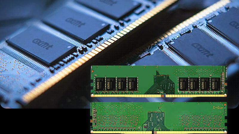
Image source: CXMT
As reported by Tom’s Hardware, citing one of the Chinese researchers, the die area of the 16-gigabit DDR5 chip made by CXMT is 40% larger than that of a comparable DDR5 chip made by South Korean Samsung Electronics. The latter is the largest memory manufacturer in the world and uses advanced lithographic technologies.
The crystal area of the DDR5 chip released by CXMT by the author of the study is determined by simple calculations. With a width and length of 8.25 mm, respectively, it is 68.06 mm2. Samsung fits its chip into more modest dimensions of 6.46 × 7.57 mm, which ultimately gives a crystal area of 48.9 mm2. This allows us to talk about the almost 40% advantage of the Samsung chip in terms of area reduction. According to TechInsights, when Micron, Samsung and SK hynix began releasing 16Gbps DDR5 chips in 2021, their die area ranged from 66.26 to 72.21 mm2, but they have since managed to reduce it. Accordingly, CXMT products at this stage of development are comparable in characteristics to first-generation DDR5 chips from foreign manufacturers, lagging behind modern solutions by four or five years. The costs of a Chinese company should also be higher, not to mention possible problems with a high level of defects. One way or another, CXMT’s partners manage to produce DDR5-6000 memory modules based on its chips, so in terms of performance they seem quite modern. The company’s Chinese clients, one way or another, are more pleased to have access to such memory than not to have it at all.