Chinese Scientists Create Advanced Solid-State Laser for Semiconductor DUV Lithography

Chinese scientists have built a compact solid-state laser system that generates coherent light with a wavelength of 193 nm, an invention that promises breakthroughs in semiconductor lithography and other technological fields.

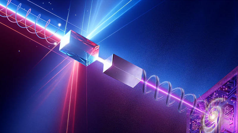
Image source: spie.org
Deep ultraviolet (DUV) lasers with high photon energy and short wavelengths are used in semiconductor lithography, high-resolution spectroscopy, precision materials processing, and quantum technologies. They are characterized by high coherence and low energy consumption compared to excimer or gas-discharge lasers, i.e., the ability to create compact installations.
Chinese scientists have made significant progress and built a compact solid-state laser system capable of generating a coherent beam with a wavelength of 193 nm, according to a paper published in the peer-reviewed scientific journal Advanced Photonics Nexus. This wavelength is crucial in semiconductor lithography, the process of etching complex patterns onto silicon wafers that form the basis of modern electronics.
The laser system operates at a pulse repetition rate of 6 kHz and uses an Yb:YAG (ytterbium-doped yttrium-aluminum garnet) crystal amplifier to produce a 1030 nm laser. The beam is split into two parts: one passes through a nonlinear crystal where it undergoes fourth harmonic generation to produce a 258 nm beam with an output power of 1.2 W; the other acts on an optical parametric amplifier to generate a 1553 nm laser with an output power of 700 mW. They are then combined in cascaded LBO (lithium triborate – LiB₃O₅) crystals to produce a 193 nm laser, achieving an average power of 70 mW with a linewidth of less than 880 MHz. Before frequency mixing, the researchers introduced a spiral phase plate into the 1553 nm beam, which generated a vortex beam with orbital angular momentum – a spiral laser beam.
The scientists have thus succeeded in producing a vortex laser beam with a wavelength of 193 nm in a solid-state setup for the first time. It can be used to seed hybrid excimer lasers on argon fluoride (ArF), in lithography of silicon wafers, in defect detection, in quantum communication and optical micromanipulation. The system offers higher efficiency and precision for semiconductor lithography and opens up new possibilities for manufacturing technologies. The generation of a vortex beam with a wavelength of 193 nm promises further breakthroughs in this field, up to a revolution in electronics production.

Recent Posts
Warhammer 40,000: Boltgun 2 Will Be Released in 2026, and You Won’t Have to Wait for a Free Printed Shooter Based on the First Part
At the Warhammer Skulls 2025 presentation, developers from the British studio Auroch Digital announced a…
The cult strategy Warhammer 40,000: Dawn of War will get a new life in 2025 thanks to a remaster – trailer and details
In line with its new strategy, Canadian studio Relic Entertainment presented a remaster of Warhammer…
Sega Announces ‘Thoughtful Restoration’ of Original Warhammer 40,000: Space Marine for New Generation of Players
Publisher Sega and developers from the Lithuanian studio SneakyBox announced a re-release of the 2011…
Xiaomi has unveiled its second electric car, the Xiaomi YU7 crossover, which is superior to the Tesla Model Y in many ways
Xiaomi has officially unveiled its second electric vehicle, the YU7 crossover in three trim levels:…
ID-Cooling DX360 Max Liquid Cooling System with Thicker Radiator
The ID-Cooling DX360 Max liquid cooling system has one, but very important difference from other…
MSI MPG Infinite X3 AI 2nd System Unit Review: All That’s Left to Do Is Play
As part of the expansion of the diversity of the "Laptops and PCs" section, it's…