Belgian Imec managed to produce record small semiconductor structures in one pass

Intel is not the only company actively purchasing High-NA EUV lithography systems from ASML. One of the first scanners of this class was located in a joint laboratory with Imec in the Netherlands, and the latter was recently able to produce test chips with record small element sizes in a single pass, proving the effectiveness of High-NA EUV equipment.

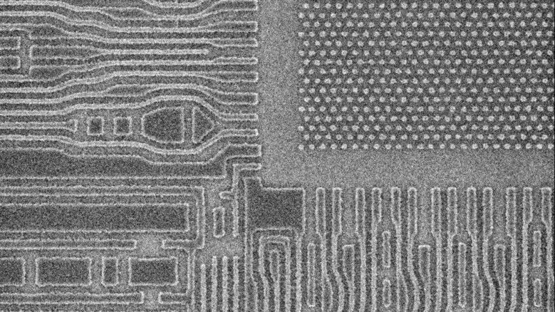
Image source: imec
Using the Twinscan EXE:5000 lithography system and equipment with new materials prepared for it by partners, Imec produced several test semiconductor structures with record small dimensions. In particular, a sample of a logic component with metallized layers demonstrated element sizes of no more than 9.5 nm with a pitch between them of 19 nm, and the distance along the vertices did not exceed 30 nm. Imec specialists managed to create a sample chip with through holes located at a distance of 30 nm from each other in one pass. The array of holes turned out to be regular; they themselves had a uniform shape and size. As part of experiments to create long two-dimensional elements, it was possible to maintain a distance between them of no more than 22 nm.
Structures replicating memory cells were also created. This is especially important given the interest in High-NA EUV equipment from large memory manufacturers such as Samsung, SK hynix and Micron. If Intel by the end of this year will receive a second lithographic scanner with a high numerical aperture value (0.55), then TSMC expects to receive only the first, and it expects to begin using such equipment in mass production no earlier than 2028, when it masters the A14 technological process.
Imec emphasizes that the success of experiments with this type of ASML equipment paves the way for the company’s customers to begin designing the products in which it will be used. Accordingly, suppliers of equipment and consumables will also take this experience into account when expanding their product range. The transition to a new class of lithographic equipment will reduce the number of passes during the exposure of photomasks, increasing the productivity of chip production lines. The only problem that remains is the high cost of such scanners, since one costs about 350 million euros.

Recent Posts
A demo of Dispatch, a comedy game about a superhero agency from the former developers of Tales from the Borderlands and The Wolf Among Us, has been released on Steam
Developers from the American AdHoc Studio, founded by former Telltale Games, Ubisoft and Night School…
Digma DP-FHD800A LCD Full HD Projector Review: A Modern Approach
When you think about a home theater, you immediately imagine bulky projectors with a bunch…
Lian Li Introduces HydroShift II LCD-C Liquid Cooling System with 360mm Radiator and Three Configurations
Lian Li has introduced a series of maintenance-free liquid cooling systems HydroShift II LCD-C. It…
Apple: App Store App Developers to Earn $406 Billion in 2024
Amid mounting pressure from U.S. regulators, Apple has released the results of an independent study…
ASRock Admits Its Motherboards Break Ryzen 9000 Processors
Following a report from YouTube channel Tech Yes City that ASRock linked Ryzen 9000 processor…
Apple to Change OS Numbering: iOS 26 to Come This Year Instead of iOS 19
Apple is preparing a large-scale rebranding of its line of operating systems. This was reported…