AI accelerators will get terabytes of memory: SanDisk plans to replace HBM with ultra-fast HBF flash memory

SanDisk will soon become independent from Western Digital, and it has big plans for the future. In particular, the company intends to develop HBF (High Bandwidth Flash) technology, which will provide AI accelerators with significantly more memory than the HBM (High Bandwidth Memory) used today.

Image source: SanDisk
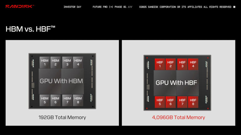
The idea may seem absurd, because NAND flash memory is traditionally much slower than DRAM, which underlies HBM. HBF is designed to solve this problem and become the optimal solution for tasks related to running already trained models (inference), rather than training neural networks. With the change of HBM generations, the available memory capacity also increases – today, accelerators from AMD and Nvidia offer 192 GB. SanDisk assures that HBF will help increase this figure by eight or even 16 times at a comparable price.
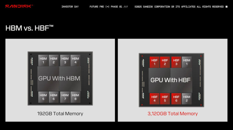

The company offers two scenarios compared to the traditional configuration with eight HBM stacks for a total of 192 GB. The first option is six HBF chips and two HBM. In this case, the total memory capacity increases to 3120 GB, or about 3 TB. The second scenario considers completely replacing HBM with HBF, which will give the accelerator 4096 GB (4 TB) of memory. This volume can completely fit a large Frontier language model with 1.8 trillion parameters and a size of 3.6 TB. In the examples given, the capacity of one HBM stack is taken as 24 GB, and HBF – 512 GB (more than 21 times higher), because NAND flash memory has a higher density.
In the HBF design, NAND flash dies are stacked on top of each other and placed above the logic die. The HBF stack, like HBM, sits on an interposer next to the GPU, CPU, or TPU, depending on where the memory is needed; the interface will require only “minor protocol changes.” The key is that HBF offers the same throughput as HBM, according to SanDisk.
In the traditional version, NAND really approaches DRAM in terms of bandwidth, but desperately loses in terms of access time. SanDisk solved this problem with a special NAND architecture, dividing the component into several areas with a greater number of data lines, which means faster access and higher performance.
The HBF architecture was developed by the company last year under the “influence of major players in the AI field.” Next, a technical advisory board will be formed, which will include the company’s partners and industry leaders; then an open standard will appear. In 2019, Japanese scientists proposed the HBN (High Bandwidth NAND) concept, and it is possible that HBF has something in common with it. Meanwhile, SanDisk has already prepared a “roadmap” describing new generations of this type of memory — both capacity and performance will increase.

Recent Posts
Nvidia to Release Simplified Blackwell Accelerator for China Costing $6,500-8,000
Nvidia is developing a stripped-down and cheaper AI accelerator based on the Blackwell architecture specifically…
German court rules that websites must have a button to reject all cookies at once
The Hanover Administrative Court has issued a ruling that tightens the protection of digital privacy…
Nuclear restructuring has begun in the US — Trump wants to step up construction of nuclear power plants
The day before, Donald Trump signed a series of executive orders that will lead to…
To Fix Problems at His Companies, Elon Musk Decides to Sleep on the Job
After widespread user complaints about unstable operation of X on Friday and Saturday, Elon Musk…
The Midnight Walk – A Spark That Will Catch a Flame. Review
PlayStation 5 played MoonHood Studio was founded in 2023, but its employees have been working…
“What do you see: craters or bulges?” – Japanese probe Resilience photographs the south pole of the Moon
The Japanese private probe Resilience has taken a high-quality photo of the Moon's south pole…