At the quarterly reporting event, TSMC management also discussed a number of conceptual issues. The company said that in the future it expects to position itself as a provider of comprehensive services for the production of chips, providing customers not just with crystals, but with finished products. The fab should include not only semiconductor manufacturing, but also related things, including lithography mask preparation, packaging and chip testing.
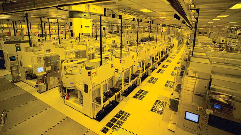
Image Source: TSMC
TSMC has been not only producing chips for some time, but also providing services in the field of packaging of complex products. And they turned out to be especially in demand in the era of the so-called “artificial intelligence boom,” since it is TSMC that packages and tests chips for Nvidia, on the basis of which it produces computation accelerators for artificial intelligence systems using other partners. Now TSMC has monopolized this type of service in the eyes of Nvidia, using the CoWoS packaging technique, but at the quarterly reporting conference, the head of TSMC C.C. Wei made it clear that it is not only expanding its existing production facilities at an accelerated pace, but is also preparing to introduce more advanced ones chip packaging methods.
According to TrendForce statistics, in the first quarter of this year, TSMC controlled about 61.7% of the global market for contract chip manufacturing services in monetary terms. The chairman of the company’s board of directors insists that, within the framework of the Foundry 2.0 concept, this chip manufacturer is ready to provide most related services, from the production of photo masks to packaging of processed crystals in a case with their further testing. As already noted, the company is actively expanding its core chip packaging capabilities. It can produce photomasks thanks to a deal with Intel, under the terms of which it last year received 10% of the shares of the core division of this company, which received relative structural independence.
According to the head of TSMC, the company’s activities in line with the Foundry 2.0 concept will allow its share in the global market for specialized services to be estimated at approximately 28%. Note that this is lower than the 61.7% that the company controls in the field of silicon wafer processing, but the number of competitors as it enters the chip testing and photomask manufacturing segments is growing. At the same time, TSMC management estimates the revenue growth potential for the entire contract industry at the end of the current year at 10%, so the company’s business itself will also benefit from such trends. Accordingly, the company’s share in this market in its broader definition will later increase. The entire semiconductor market this year, with the exception of the memory segment, will grow by the same 10%, according to TSMC. The company’s chief financial officer, Wendell Huang, added that TSMC’s decision to introduce the “Foundry 2.0” concept came as some vertically integrated chip developers entered the contract services market. This definition suggests Intel with its IDM 2.0 concept.