The experience of the Japanese company Fujitsu in the development of processors and supercomputers is great and multifaceted. For a long time, the main architecture for Fujitsu solutions was SPARC64, but times are changing: in 2018, the company announced the development of its own processor based on the Arm architecture. Today we know this chip under the name A64FX.
In 2020, the Japanese Fugaku cluster based on 48-core A64FX with integrated HBM memory and interconnect took first place in the TOP500 ranking with a result of 537.2 Pflops. However, these processors, which still work well not only in Fugaku, but also in other supercomputers, can hardly be called truly universal and affordable.
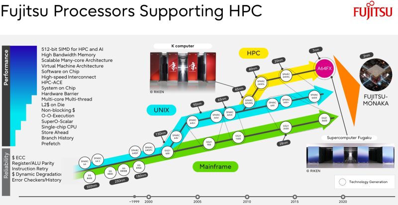
Image source: Fujitsu
Fujitsu is well aware of the importance of architectural innovations and the changing IT landscape. Therefore, the company also announced the development of a new server processor, codenamed MONAKA, for which it intends to double performance and energy efficiency, as well as take into account the growing popularity of AI tasks. And just recently, Fujitsu for the first time spoke in more detail about the technical features of future CPUs.
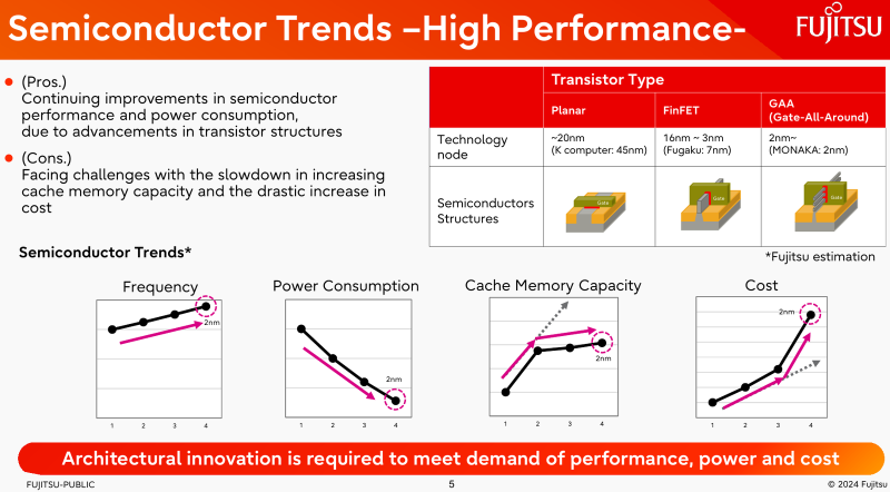
First, the developers of the new processor are well aware of the limitations imposed by current transistor technology. It seems that all or almost all the juice has been squeezed out of FinFET and its analogues and this technology is not suitable for breakthrough solutions of the new generation. MONAKA processors will use a new type of gate transistor, the so-called GAA (Gate-all-Around). It seems that we are talking about technology that Samsung is developing and intends to introduce into production next year as part of the 2nm SF2 process.
The introduction of 2-nm GAA transistors will reduce parasitic capacitance, which means achieving higher clock frequencies with a lower supply voltage. At the same time, the new technology will be applied not only in processor cores, but also in cache memory assemblies, also designed using Fujitsu’s own tools.
Secondly, MONAKA is initially designed as a modular processor. In the center there will be an IO crystal containing DDR5 (12 channels) and PCI Express 6.0/CXL 3.0 controllers. It will be surrounded by assemblies of 5nm SRAM cache memory chips and 2nm chips with processor cores located on top. The vertical connection will be provided by TSV technology, and the horizontal connection will be provided by a silicon interposer substrate. In fact, we are talking about a 3D layout.
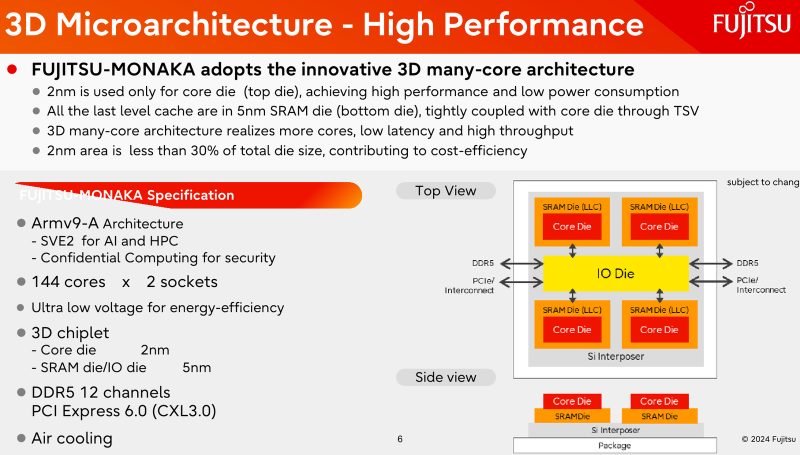
The 12-channel memory subsystem will ensure there are no bottlenecks: the A64FX had no problems with bandwidth thanks to the use of HBM2, but the memory itself was limited to 32 GB. But MONAKA will not have problems with expansion – both using classic DIMM modules and through CXL memory banks, fortunately, the PCIe 6.0 version with a bandwidth of 256 GB/s in x16 mode is immediately taken as the basis. How many lines there will be has not yet been specified.
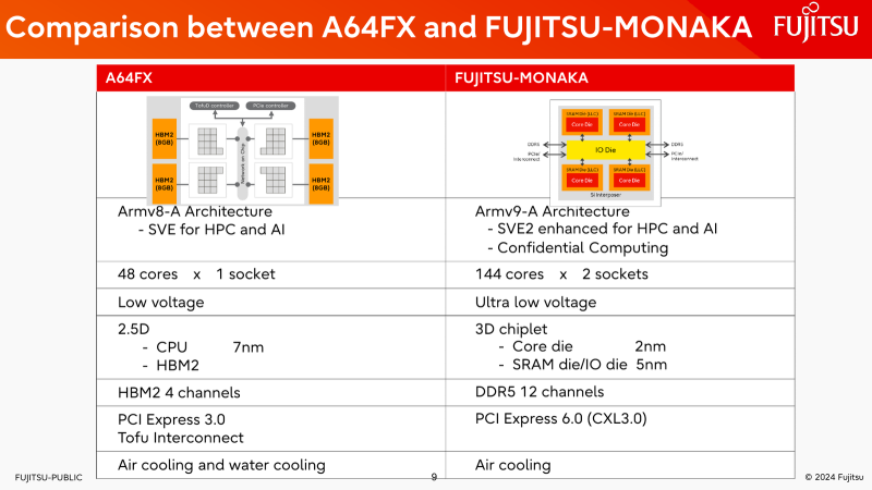
The new platform is initially designed as a two-socket platform, and Fujitsu is also not being modest in the number of cores: MONAKA processors will have 144 cores, and thanks to the new 2nm process technology they will not be so hot. Air cooling is enough for them, the creators say. The processors will receive the Armv9-A instruction set with SVE2 vector extensions and Confidential Computing technology. Most likely, it won’t be possible this time without custom instructions.
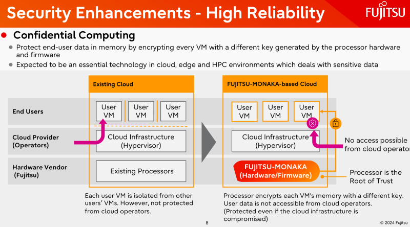
The latter is especially important due to the fact that MONAKA is intended not only for the HPC market, but also for use in cloud environments. The confidential computing subsystem allows you to encrypt the contents of each virtual machine with its own key, so that even the owners of the data center will not have access to the insides of the VM. However, modern HPC systems are increasingly using the cloud approach to access resources.
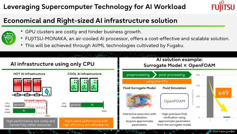
Despite the popularity of GPUs and other specialized accelerators, Fujitsu believes that heterogeneous architecture has significant disadvantages – it is noticeably more expensive, especially taking into account the pricing policy of manufacturers, is prone to incomplete utilization of resources, and is also not very economical and often requires specific cooling systems. The company believes that the homogeneous MONAKA architecture does not have these shortcomings and, in combination with Fujitsu software, can successfully handle AI workloads.
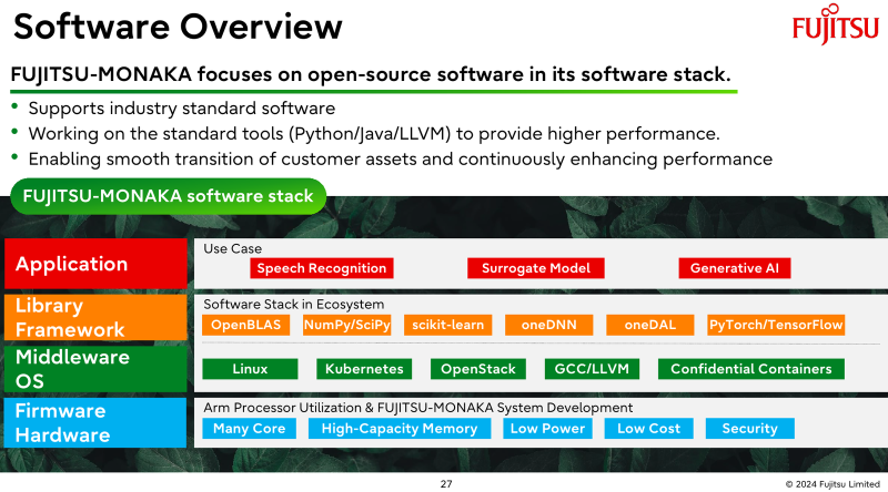
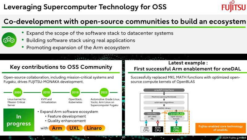
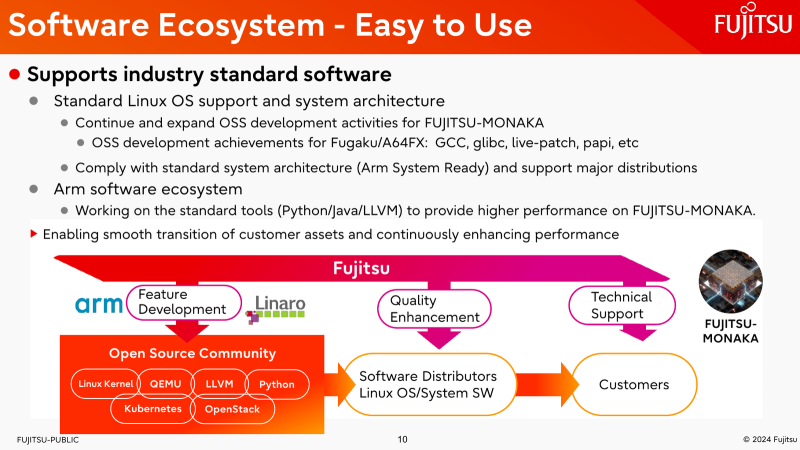
On the software side, Fujitsu relies heavily on open source solutions. MONAKA processors will meet Arm System Ready standards and will receive full support for Linux and related tools, in particular, GCC, glibc, live-patch, papi, etc. Development is being carried out in close collaboration with Linaro, an organization dedicated to consolidating open source software for Arm, as well as the UXL alliance. For MONAKA, the company will prepare, for example, an optimized OpenBLAS library.
Fujitsu also pays attention to the environment: let us remind you that one of the main features of the new processor will be its efficiency, which meets the goals of the Japanese national NEDO program, which aims to achieve a 40% reduction in data center energy consumption by 2030.
As for the start of deliveries of MONAKA, everything is going according to plan: the first batches of new processors will find their place in servers and computing nodes as early as 2027. This is consistent with the PCI Express development cycle, according to which PCIe 6.0 solutions should not be expected to hit the market until 2025.