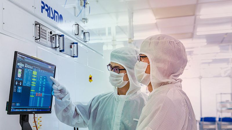
The most advanced 7nm chips produced by the Chinese SMIC for Huawei are generally believed to be manufactured using DUV equipment from the Netherlands’ ASML. Judging by the update of the catalog of domestic equipment available to Chinese manufacturers, they will soon have the opportunity to produce 8-nm products regardless of their access to foreign lithographic systems.

Image source: AMEC
This conclusion is reached by the TrendForce resource, citing the publication by the Ministry of Industry and Information Technology of the People’s Republic of China of an updated catalog, which was compiled to promote technical equipment of Chinese origin.
It is not specified at what stage of readiness for entering the market the corresponding system is, but the document emphasizes that it will allow the production of chips with an interlayer alignment accuracy of no more than 8 nm. The resolution of such equipment does not exceed 65 nm; it uses a laser with a wavelength of 248 nm and silicon wafers with a standard size of 300 mm. In other words, the appropriate equipment allows you to create 8-nm chips without switching to ultra-hard ultraviolet (EUV) lasers.
It is assumed that the Chinese companies AMEC and SMEE, as well as representatives of the scientific community of the PRC, took part in the development of such a lithographic system. This month, the Netherlands imposed further restrictions on the supply of DUV lithography scanners made by ASML to China. If Chinese manufacturers manage to launch the production of DUV scanners for the production of 8-nm products, then the local semiconductor industry will no longer depend on the USA, the Netherlands and Japan for some part of the product range covered.