Just 4 months after the launch of the 9th generation TLC V-NAND, Samsung announced the start of mass production of similar QLC memory, offering the market a wider range of advanced storage solutions. The new memory delivers optimal performance for a wide range of applications, including artificial intelligence (AI) workloads.
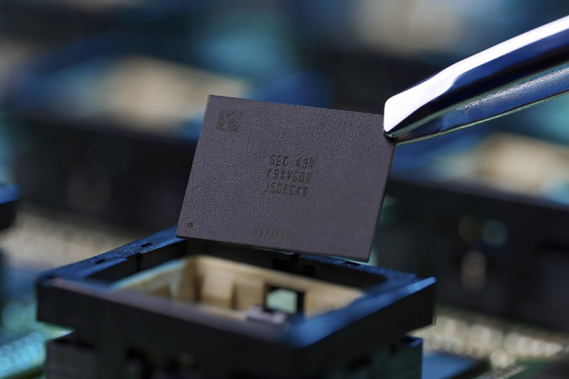
Image Source: Samsung Electronics
Samsung Electronics announced the start of mass production of the 9th generation of vertical NAND memory (V-NAND) with four bits per cell (Quad Level Cell, QLC) with a capacity of 1 Tbit. “The successful mass production launch of 9th generation QLC V-NAND just four months after the TLC version allows us to offer a full line of advanced SSD solutions to meet the needs of the AI era,” said SungHoi Hur, executive vice-president. -President and Head of Samsung’s Flash Memory and Technology Division.
Samsung plans to expand the application of 9th generation QLC V-NAND from branded consumer products to mobile universal flash memory (UFS), SSDs for client PCs and servers, including solutions for cloud service providers. The new generation of memory is distinguished by a number of technological capabilities, or better yet, breakthroughs. Thus, Channel Hole Etching (channel etching technology) from Samsung made it possible to achieve the maximum number of layers in the industry with a two-level structure. In doing so, leveraging the experience gained from developing the Triple Level Cell (TLC) 9th Generation V-NAND, Samsung has optimized cell and peripheral circuit area to achieve an industry-leading bit density that is approximately 86% higher than QLC V -NAND of the previous generation.
In addition to high density, the ninth generation QLC V-NAND features increased performance and reliability thanks to Designed Mold, Predictive Program and Low-Power Design technologies. Designed Mold technology adjusts the distance between Word Lines (WL) to ensure uniformity and optimize cell performance across all layers. Predictive Program technology predicts and controls changes in cell state to minimize unnecessary actions. As a result, Samsung was able to double the write speed and increase the data input/output speed by 60%, and reduce power consumption when reading and writing data by approximately 30% and 50%, respectively, thanks to the use of Low-Power Design.