TSMC managed to get ahead of Intel in launching mass production of EUV equipment, but in the more advanced High-NA EUV segment, the company lagged behind its American competitor. Intel already uses ASML’s High-NA EUV machine for research and development, and TSMC will begin installing the first such scanner only this month, DigiTimes and United Daily News have learned.
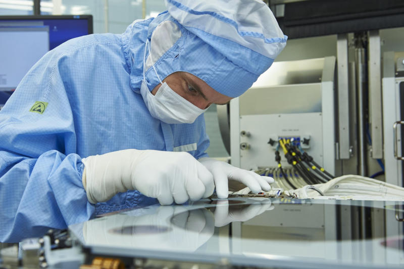
Image source: asml.com
The first ASML Twinscan EXE:5000 ultra-hard ultraviolet high numerical aperture (High-NA EUV) unit, built specifically for R&D applications, will be installed at TSMC’s Hsinchu facility in Taiwan. The world’s largest semiconductor contractor will begin receiving machine components in September, followed by several months of assembly and calibration before testing next-generation semiconductor technology.
TSMC’s advanced N2 (2 nm class) and A16 (1.6 nm class) process technologies will run exclusively on low NA 0.33 EUV hardware. The High-NA EUV scanner (0.55 numerical aperture) will be used for the A14 process technology (1.4 nm class) approximately in 2028, although the company has not yet made official statements on this matter. But its implementation will cause additional difficulties for both manufacturers and developers, so TSMC is in no hurry to deploy such scanners.
Another argument not in favor of the new generation machines is their price, which, as Kevin Zhang, responsible for the development of new technological processes at TSMC, said, he liked less than the performance. Each High-NA machine costs about $400 million, although company president C.C. Wei managed to negotiate a discount of almost 20% when purchasing several units at once. Given that TSMC is the leading EUV lithography manufacturer and has 65% of ASML’s global EUV capacity, the Dutch manufacturer is naturally inclined to make deals with a plant that is one of its largest customers.