Japan’s National Institute of Advanced Industrial Science and Technology (AIST) and Intel will establish a new research and development center in Japan. It will be focused on developing technical processes for advanced chips based on EUV lithography, Nikkei writes, citing informed sources.
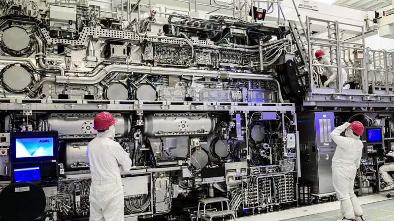
Image Source: Intel
The project, which will cost hundreds of millions of dollars ($273 million per EUV lithography unit), is expected to take 3–5 years. This center will install advanced EUV equipment on which Japanese companies will be able to debug their technologies. The creation of the new center will provide Japanese enterprises with the opportunity, in collaboration with AIST and Intel, to develop and implement the latest technological processes, which will increase their competitiveness in the global market.
Japanese companies now have to turn to foreign research centers such as Belgium’s IMEC to gain access to EUV equipment to develop new products. Establishing a research center in Japan will allow local companies to reduce their dependence on foreign resources, which will help speed up the development of new chips and increase the competitiveness of the domestic semiconductor industry.
In turn, Nikkei argues that the joint research and development center between Intel and AIST is strategically important because it will eliminate the need for Japan to go to U.S. regulators to transfer research data and technology from the United States amid tightening export restrictions.