We have already mentioned before that optical phenomena are usually perceived as linear; it is the consideration of light flows as straight segments that underlies classical optics with its refractions and reflections strictly aligned along a protractor. However, this is true only in the most general, everyday approximation; as long as the response of the substance in which the flow of photons propagates depends linearly on the magnitude of the electromagnetic field of this flow. In the second half of the 19th century, with the experiments of Faraday and Kerr, the study of nonlinear optics began: scientists began to realize that a portion of light radiation passing through a certain medium affects this medium itself, changing its properties – and thereby making simple mechanistic ideas about all the processes occurring there incorrect. . Another question is that before the advent of lasers, the intensities of the photon fluxes available to experimenters were relatively small, but already at the beginning of the 20th century, against the backdrop of the rapid development of quantum theory, it became clear that photons as quantum particles are simply obliged to behave in a significantly nonlinear manner at significant energies way.
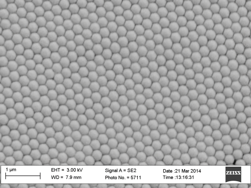
Two-dimensional photonic crystal made of synthetic polymer under an electron microscope (source: Wikimedia Commons)
Photonic crystals, which were already discussed in our previous material, are solid-state media with a periodic structure, the electrical properties of which (and above all, the dielectric constant, which ultimately determines the local refractive index) change at distances comparable to the wavelength of the propagating radiation through them. A living example of such a structure, quite adequate to the topic of microelectronics, is Bragg mirrors, thanks to which, in principle, the creation of EUV photolithographs is possible. There, multilayer quarter-wave films (in thickness) with alternating large and small refractive indices provide a significant, several orders of magnitude, increase in the intensity of reflected X-ray radiation – due to multiple interference mutual reinforcement of in-phase (in-phase) waves.
If the mirror of an EUV photolithograph behaved as an element of a linear optical circuit, the intensity of the X-ray flux reflected from it would be no more than 0.14% of the original – the energy of the corresponding photons is so high that it is energetically more favorable for them to be absorbed in the thickness of the substance than to be reflected from its surface . At the same time, a nonlinear structure of fifty alternating layers of molybdenum and silicon, each approximately 3.4 nm thick, provides – due to amplifying interference – the intensity of reflected radiation at a level of 70% of the original one. In accordance with the same principle of Bragg diffraction, photonic crystals change the rules for the propagation of light in their thickness, creating for photons (more precisely, for certain photon energies) allowed and forbidden zones – similar to those that exist for electrons in semiconductors. In combination with the high intensity of laser radiation passing through the photonic crystal, which guarantees the manifestation of nonlinear optical effects, it becomes possible to very delicately and effectively control the light flux – something that developers of purely optical logic circuits readily take advantage of.
⇡#Thin film constructivism
A free electron that moves in the crystal structure of a semiconductor is influenced by the nodes of this structure – neutral atoms and/or ions; more precisely, the electromagnetic fields generated by those. A photon, like a particle that has no electrical charge and flies at the speed of light, simply “does not feel” the structure of a crystal: after all, its wavelength is much greater than the characteristic pitch of the crystal lattice. From here it is clear why solids with a periodic structure, which still affects the quanta of electromagnetic radiation, provoking their constructive/destructive interference, are called “photonic crystals”. It is precisely in such a medium that it becomes inhomogeneous for it that the photon is able to change the characteristics of its movement in response to its changeable structural features (and not simply reacting to some indicator uniform for its entire thickness, such as the refractive index) – exactly the same sense in which a free electron “feels” the influence of the nodes of the crystal lattice of a semiconductor.
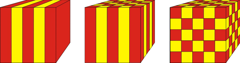
Schematic representation of the spatial structure of one-, two- and three-dimensional photonic crystals (source: Wikimedia Commons)
Since the nature of the propagation of light inside a photonic crystal depends on exactly how the interference of photons occurs in its thickness, “allowed” and “forbidden” energies, or radiation frequencies, arise in a completely natural way: the first – as a manifestation of the constructive interference of light waves on a periodic structure environment; the latter are destructive. Only light with allowed wavelengths passes through a photonic crystal or its individual sections (yes, in neighboring regions of the medium of the same sample, different wavelengths can be allowed and forbidden – in our previous article we already showed this using the example of a two-dimensional photonic crystal). In extreme cases, we can talk about “photonic conductors” and “photonic insulators” (the definition “photonic dielectric” would sound incorrect: although a photon is a quantum of electromagnetic radiation, it has no electric charge). Photonic crystals – conductors have extremely wide band gaps and transmit radiation of an impressive range of energies (wavelengths) through themselves with minimal losses, while insulating crystals, on the contrary, are characterized by wide band gaps – and therefore are practically opaque. Accordingly, “photonic semiconductors” have a bandgap width that is intermediate between the two indicated extremes, and such media (which, in fact, are photonic crystals) are suitable for the formation of elementary units of logical circuits – diodes and transistors.
Let us use a simple example of a one-dimensional photonic crystal to explain exactly how allowed and forbidden bands arise. Such a crystal is most easily realized in the form of a selection of thin films tightly adjacent to one another, the refractive indices of which alternate: strong – weak, strong – weak. If each of these films extends in thickness to a quarter of the wavelength of light transmitted through them, the entire structure as a whole begins to extremely resemble the multilayer Bragg mirror already familiar to readers of material on EUV photolithography – with the only exception that in this case the radiation flux is not reflected from the optical system, but passes through it, and the wavelengths of the electromagnetic interaction quanta are calculated not in the first tens of nanometers, but already in the hundreds.
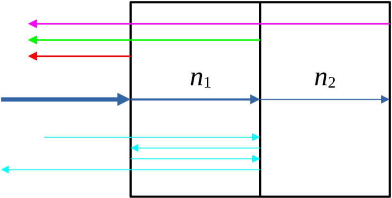
Paths of individual light rays in a two-cell one-dimensional photonic crystal (see explanation in the text)
В простейшем случае рассмотрим фотонный кристалл всего из двух плёнок, с обеих сторон ограниченных воздухом (показатель преломления которого принимаем ровно за 1), причём первая плёнка пусть преломляет свет сильнее, чем вторая (n1 > n2 > 1). A beam incident on such a photonic crystal will partially pass through it, losing a certain fraction of its energy (the fraction of its constituent photons) at each interface between media with different refractive indices, and partially will be reflected strictly in the opposite direction. By the way, let us take into account only rays perpendicular to the interfaces between the media, so as not to take into account additional reflections from the side walls of the cells. In addition, rays that have changed direction several times will go back: say, having reached the interface between the media n1 and n2 – reflected back and again reflected from the interface of n1 with air – again reaching the interface of n1 with n2 and once again reflected back, but now already out. This turns out to be three complete re-reflections (with a loss of beam intensity at each, of course) – or maybe five, or seven, or more. However, the most significant contribution to the intensity of the light beam that comes back from such a two-cell photonic crystal will be made by rays reflected once from each of the three main boundaries: from air with a medium with a refractive index n1, from the interface between media n1 and n2, and also from the boundary n2 and outside air.
In order for these three beams to form with mutual amplification – producing, in fact, the effect for which the direction of photonic crystals is developed – they must turn out to be in phase, i.e. sinusoids, which represent the change in their phase depending on the path traveled, must in match exactly. Let us recall (as we already did when analyzing the operating principle of the Bragg mirror), that if a beam from a medium with a lower optical density hits the boundary with a medium with a higher optical density (higher refractive index), then the phase of the reflected light changes to π, and if a beam from an optically denser medium hits the boundary with a less dense one, such a phase change does not occur.
Значит, первый луч — от границы между воздухом и средой с показателем преломления n1 — отразится с переменой фазы на π. Второй луч пройдёт эту границу и отразится от следующей, между средами n1 и n2, и, поскольку n1 > N2, no phase change will occur. Let us remind you that we took a photonic crystal from films a quarter of a wavelength thick, so the second ray, passing back and forth through the first film, will lag behind the first by exactly half a wavelength, i.e., by phase π. Thus, the quarter-wave film alone provides in-phase (and, therefore, amplification) of the light reflected by it, the wavelength of which is exactly four times its thickness. If the light is non-monochromatic, photons with other wavelengths will, of course, also be reflected from the interfaces between the media, but due to the lack of in-phase, the corresponding fluxes will not increase. In other words, a one-dimensional photonic crystal acts as an ultra-narrowband filter, selectively amplifying a very limited portion of the original light flux.
⇡#We will filter
If you now look at a photonic crystal (also called a distributed Bragg reflector for obvious reasons) as a light filter, i.e., take care of the characteristics of the light transmitted by it, it will immediately become obvious that the band gap for it covers those wavelengths whose radiation Due to the mechanism just described, it is completely (or at least significantly) reflected back – and does not pass through. In order for the band gap to be precisely an extended zone, and not a fixed wavelength, for which the films forming a photonic crystal are quarter-wavelength, media with significantly different refractive indices are taken, and their layers are made ultra-thin and numerous – so that for many adjacent wavelengths the in-phase condition is satisfied undergoing multiple reflections and emitting light streams in the opposite direction.
Electron micrograph of a one-dimensional photonic crystal with a defect formed by alternating layers of titanium dioxide and silicon dioxide (source: Technical University Ostrava)
By varying the thickness, number of layers and refractive indices for them, engineers have learned to create distributed Bragg reflectors with very wide band gaps, which essentially work like optical filters – transmitting (with a certain reduction in intensity, of course) only part of the light incident on them in a spectral range wide several hundred nanometers. These filters are quite broadband, but through a simple procedure – introducing defects into them – it turns out to be extremely easy to obtain phononic crystals with a bandwidth of literally a few nanometers, or even less.
For one-dimensional structures, a defect usually represents a violation of the order of alternation of layers with different refractive indices. The idea here is simple: two quarter-wave films of identical optical properties, placed next to each other, form one section with a constant refractive index, but with an extension of half the wavelength. This violates the in-phase condition: the waves reflected from the boundaries of the “defective” section will be out of phase with the others – and for a given wavelength, the reflection of light in the photonic crystal will be blocked, and, consequently, the flow will pass through this structure with minimal losses.
Moving from one-dimensional photonic crystals to two- and three-dimensional ones, we can generalize their definition to a periodically structured dielectric, which forms a periodically inhomogeneous distribution of dielectric constant in space (which, recall, ultimately determines the refractive index of the medium). It is this spatially ordered distribution that is responsible for the formation of the band structure of the energy levels of photons – in the same sense in which the atoms and ions of the most common semiconductor located at the nodes of the crystal lattice form a three-dimensional periodic distribution of electric potential for electrons, creating allowed and forbidden energy bands .
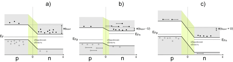
Energy diagram of a pn junction: a) in a state of equilibrium; b) with applied forward voltage; c) with reverse voltage applied (source: Wikimedia Commons)
Let us recall on what principle the simplest semiconductor device based on a pn junction works. Such a device consists of two physically touching volumes of a semiconductor, one of which is saturated with excess electrons (particles with a negative electrical charge; and therefore denoted as n, from “negative”), and the other, on the contrary, experiences a shortage of electrons in the outer atomic shells (which can be interpreted as its saturation with conditional “holes” – carriers of positive charge; p, “positive”). On both sides of the boundary of contact of such volumes, a p-n junction zone is formed – due to the fact that electrons from where there is an excess of them (n-type zone), due to thermal movement, enter the volume with their shortage (p-type zone) . And there they quickly “recombine with holes,” that is, they occupy vacant positions on the outer shells of the corresponding atoms. In the same way, holes from the p-region “move” to a thin (about 100 nm) layer beyond the boundary with the n-region – and there they recombine with excess free electrons.
As a result, at the junction of the p- and n-volumes of the semiconductor, a blocking layer is formed, in which, on the sides of the boundary, the concentration of the corresponding charges is lower than the initial one. Since there are fewer electrons on the side of the n-region in the blocking layer than on average over its volume (since they tend to diffuse into the neighboring p-region and recombine with holes there), an excess (compared to the main volume) is formed on the n-side of the junction of semiconductor volumes n-zone) positive charge. On the contrary, on the p-region side the hole concentration is already reduced for the same reason – an excess negative charge arises here. This potential difference forms an electric field at the boundary of the p- and n-regions – which, in turn, begins to repel holes from the junction zone deep into the p-region, and electrons, accordingly, deep into the n-region.
That is, if initially, at the first contact of the p- and n-mediums, electrons and holes diffused freely across the boundary, then after a fairly short time the blocking layer will form a certain potential barrier. This means that to overcome it, it will be necessary to apply to the sample, which consists of adjacent p- and n-regions, such a potential difference that would help charge carriers move in the desired direction – this is called direct inclusion of the p-n junction, leading to an increase in conductivity barrier layer and activation of the electrical charge transmission channel. And vice versa, if we apply a potential difference with the opposite sign – the reverse switching on of the p-n junction – the potential barrier will become even higher than before, so that the current is guaranteed not to flow through the circuit (if the voltage is not brought to the breakdown level, of course – but this is the limiting case we not considered in application to normally functioning semiconductor devices).
⇡#Down with linearity!
Such a detailed, albeit without formulas, explanation of the basic principle of operation of semiconductor devices based on the p-n junction effect will allow, I would like to believe, a better understanding of the implementation of similar processes in photonic crystals. Instead of semiconductors with an excess of electrons and holes, to form a structure similar to a p-n junction, photonic crystals with different band gaps are taken – in the first, such a zone will be located lower along the energy axis, in the second, higher. Then, if photons move through the second crystal to the first, it is energetically favorable for them to continue moving – the flow of light will pass through the boundary. If you direct light in the opposite direction, through a photonic crystal with a lower band gap to the second one, the radiation flow will be blocked. A more complex scheme involves the use of optically nonlinear media in the role of photonic crystals: if you select materials for the first and second of them so that with increasing light intensity the band gap in the first decreases even more, and in the second, on the contrary, increases, then the “diode” effect Such a scheme will not only be preserved (transition of photons from the second crystal to the first is possible, but vice versa is not possible), but will also increase with increasing concentration of photons in the beam.
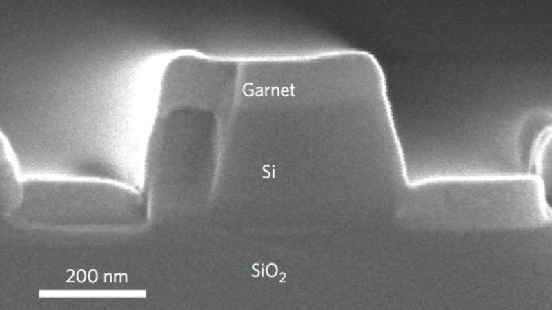
Photonic diode implemented using classical photolithography methods using one of the varieties of garnet on a silicon basis (source: MIT)
«Photonic diodes” based on one of the varieties of artificially grown garnet were proposed back in 2011 by researchers from the Massachusetts Institute of Technology. At that time, there was no talk of creating all-optical logic circuits—it was necessary to ensure complete suppression of spurious reflections in hybrid electro-optical systems with semiconductor lasers. The developers managed to implement a photonic crystal with strictly one-way transmission in a given wavelength range directly on a silicon substrate – and since a single diode can be organized in this way, then in principle there is nothing stopping you from building logical circuits of any level of complexity. Moreover, photonic crystals are capable of acting not only as logic elements, but also as waveguides for redirecting light flows between them – and this, in turn, opens up prospects for significantly reducing the area of purely optical logic circuits.
We have already explained earlier what the problem is with traditional waveguides, through which the light flux propagates due to total internal reflection from the walls. This physical phenomenon is realized only at certain angles of incidence of the beam on the reflecting surface, which means that arbitrary bending of such waveguides – at 90°, and even more so at sharp angles – will not work: light will not overcome such a bend. In the case of photonic crystals, there is no such problem: the propagation of the light flux in them is determined by the interference of waves scattered by elements of the periodic structure and/or its defects. Accordingly, the location of defects can be selected – calculated on the basis of Maxwell’s equations – in such a way that the light that reaches the “dead end” of the photonic crystal acting as a waveguide seems to turn around at a given angle (straight or even acute) and continues moving along the other arm of that the same waveguide. Thus, in the course of the practical implementation of two-dimensional photonic crystals (for example, by the method of ordered etching of “air holes” in a silicon substrate, discussed in the previous material), it is possible, by introducing carefully calculated defects into the ordered structure, to form both elements of logical circuits and connecting them for signal transmission waveguides.
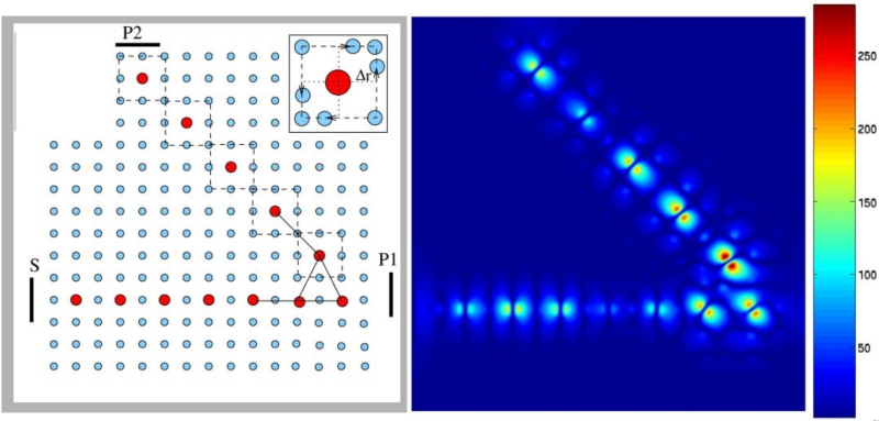
One of the possible schemes for organizing defects in a two-dimensional photonic crystal for turning the light flux by 45° (left) and the intensity distribution of the photon beam in the resulting waveguide (source: NASA Ames Research Center)
Described back in 1987 by American physicists Eli Yablonovitch and Sajeev John, photonic crystals are also known in nature: examples include natural mother-of-pearl, scales on the wings of a swallowtail butterfly, or semi-precious opal stones. The production of photonic crystals for computing systems is still carried out mostly in laboratory conditions, since scaling production towards large-scale production is associated with a significant increase in the likelihood of the appearance of unplanned irregularities (not to be confused with defects introduced strictly according to calculation!) in the structure of these complex media. Three-dimensional photonic crystals are especially capricious in this regard – although the principles of their creation have been defined for a long time, achieving high uniformity of periodic microstructures on a scale of even cubic millimeters turns out to be extremely difficult. The cost of a high-period macroscopic photonic crystal (the basis for creating a promising pure light logic circuit) is still prohibitive, and therefore, against the background of the rather vigorous progress of the traditional semiconductor industry, the direction of photonics seems somewhat stagnant.
For now, hybrid optoelectronic devices continue to be the most practical – like the integrated circuit proposed back in 2015 with 70 million semiconductor transistors and 850 optical components, made according to “45-nm” production standards, or those used in universal read-write heads of magnetic disk drives HAMR photonic waveguide crystals that “bend” the light flux by 90°. However, experts associate the real flourishing of photonics with the development of corresponding quantum computing. After all, a photon is a quantum of electromagnetic interaction; Why try to direct these particles along the classical paths trodden by electrons, if you can immediately bet on their quantum nature? Compared to other methods of implementing quantum computing, photonic computing has an undeniable advantage: longer coherence times for pairs of particles in a state of quantum entanglement. Moreover, this coherence (at least in theory) can be maintained at room temperature, which in itself provides a photonic quantum computer with significant benefits in terms of compactness and energy consumption.
Optical fiber formed by waveguides of photonic crystals with a diameter of each 4 microns (source: Wikimedia Commons)
However, even when applied to classical, non-quantum computing, photonics continues to be an attractive field – due to the highest (maximum in nature) speed of light of information carriers in photonic circuits and their modest energy consumption compared to semiconductor devices. In order for KOICs (quantum-optical integrated circuits) to equal the commercial attractiveness of modern VLSIs (ultra-large-scale integrated circuits on semiconductors), many more engineering problems will have to be solved – including the rather significant dependence of the optical properties of the materials used today for waveguides and photonic crystals on temperature, a noticeable level of energy loss when a light beam passes through a long series of waveguides and logical circuits, ensuring strict periodicity of structures directing photon flows on macroscopic scales, etc. In addition, we should not forget that silicon, for all its advantages, although suitable for mass production of COIS , is a material with an indirect bandgap, and therefore radiation sources (lasers) for purely optical computing circuits will have to be made separately from these structures themselves, which further complicates the production processes, packaging of such microcircuits and their operation. Nevertheless, the main self-fulfilling prophecy of the semiconductor industry, Moore’s law, is being fulfilled more and more clearly as time goes on, so photonics has a good chance of settling down and establishing itself as an alternative to classical microelectronics in the next decade. ByAt least, the economic prerequisites for this will become more and more obvious from year to year.
⇡#Related materials
China has found a way to mass produce optical chips that the United States will not suppress with sanctions.
The Chinese have created a metamaterial to slow down light by 10,000 times – this will help processors switch from electrons to photons.
The developer of photonic solutions Lightmatter received another $155 million for development.
Intel showed an experimental RISC processor for DARPA: 528 threads on 8 cores + integrated photonics.
Microsoft presented the world’s first analog optical computer – photons will handle optimization tasks.