The Belgian research center Imec and ASML recently signed a five-year agreement, under which the Dutch lithography equipment manufacturer will provide Imec with a full range of cutting-edge tools for chip production and quality control. The partnership will enable the development and industrialization of sub-2 nm processes down to the atomic level.
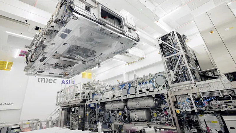
Image source: imec
Imec researchers previously used cutting-edge lithography equipment at ASML’s home site in Veldhoven, the Netherlands. The agreement will bring similar equipment to Imec, making work easier and more streamlined for the center’s staff and their partners in academia and industry.
ASML’s latest equipment, including a $350 million High-NA EUV scanner, will be integrated into the NanoIC pilot silicon wafer processing line in Belgium. The EU and Flemish authorities previously invested in the NanoIC line. In fact, ASML’s delivery will be largely financed by European funds and programs aimed at developing advanced semiconductor technologies.
Along with the Twinscan EXE (High-NA 0.55) scanner, Imec will receive a Twinscan NXE (NA 0.33), a Twinscan NXT (DUV, 193 nm), ASML YieldStar optical metrology tools and single- and multi-beam HMI inspection tools. The Belgians will receive all the best ASML toys, and in return will transfer lithographic production technologies with process standards of less than 2 nm for industrial implementation and will develop the process technologies of the next two decades.
A great complement to the joint work on next-generation process nodes for logic chips with a process technology of less than 2 nm will be cooperation in the field of DRAM production technologies, silicon photonics and advanced chip packaging solutions – all of which are in great demand by the modern semiconductor industry, which has clearly approached the technological barrier of classical process technologies.