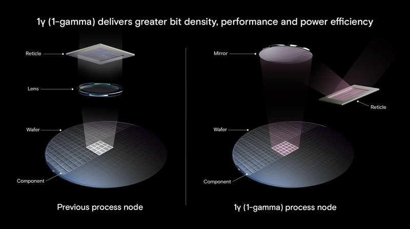
South Korean sources report that Micron has no plans to expand the use of EUV scanners in memory production in the foreseeable future. The loud announcement of the world’s first Micron DDR5 chips of the 1γ generation using EUV lithography (wavelength 13.5 nm) turned out to be a kind of psychological attack on competitors. In the future, the company intends to rely on the mass use of classic 193-nm scanners in DRAM production.
Image source: Micron
Chosun Biz reported that when producing Micron DDR5 memory of the 1γ (gamma) generation, only one layer out of several dozen is processed using an EUV scanner. All other layers are created using argon-fluoride excimer lasers (ArF) with immersion in liquid (so-called immersion lithography for increasing resolution). Thus, the company continues to use a multi-mask approach – the use of several photomasks for each layer of chips instead of a single template in EUV lithography. This increases the number of technological stages in the processing of each silicon wafer with memory, and therefore the cost of production.
The publication notes that the multi-mask approach can be justified if it serves as an alternative to EUV scanners for processing 1-3 layers of chips. However, if more layers need to be processed using EUV, relying on ArF lithography will cost the manufacturer significantly more, which will make the product less competitive (more expensive) in the long run.
Samsung and SK Hynix are already planning to use EUV scanners to process more than five chip layers (currently HBM memory), which will make Micron look seriously behind. If Chosun Biz’s information is correct, the company will use EUV scanners for a long time to only process one critical layer, relying on 193nm scanners for everything else.