Kioxia announced 332-layer 3D NAND this month, so Korea’s SK hynix can’t claim the record, although it already launched 321-layer production in November, not to mention China’s YMTC with its 294 layers. Now it has become known that both Samsung and SK hynix will have to license YMTC’s technology to produce 400-layer 3D NAND.
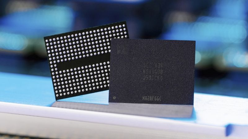
Image Source: Samsung Electronics
At least, this is what ZDNet Korea claims, which reported on the successful completion of negotiations between Samsung Electronics and YMTC. The Chinese manufacturer will provide the Korean with licensing rights to produce 10th-generation 3D NAND memory using hybrid fusion technology, which in YMTC terminology is called Xtacking and was patented earlier. More precisely, YMTC itself received a license to use this method of combining two silicon wafers from Xperi back in 2021, and was the first among flash memory manufacturers to begin using it in practice.
Samsung Electronics expects to use this technology in the production of its own 3D NAND memory chips with more than 400 layers from the second half of this year, so the corresponding license agreement with YMTC was signed in advance.
Rival SK hynix is not expected to start producing 400-layer memory until next year, but it started producing 321-layer chips last November, so it is currently ahead of Samsung with its 286-layer memory. Korean manufacturers are expected to need to license technology from YMTC to increase the number of layers to more than 400.