The topic of Samsung products complying with Nvidia’s requirements for memory chips of the HBM3 and HBM3E types is not leaving the news feeds, and new data suggests that the first type of memory has already received customer approval, and the second should do so within the next four months. However, there is a risk that this long-awaited event will occur as early as 2025.
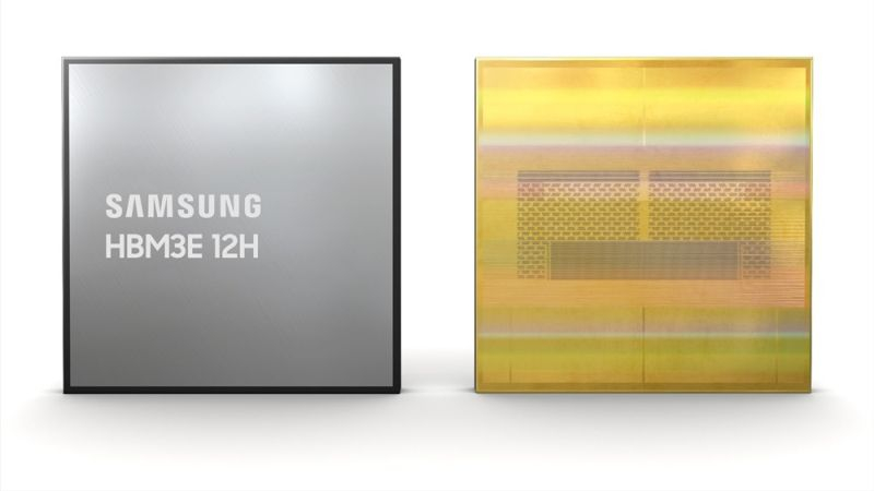
Image Source: Samsung Electronics
Bloomberg reports with renewed vigor about the misadventures of Samsung Electronics in this area. According to informed sources, Samsung has already received Nvidia’s approval for the use of its HBM3 chips in the products of this graphics processor developer, and the first product with this combination of components could be the H20 computing accelerator, created specifically for the Chinese market taking into account current American sanctions.
As for Samsung’s more modern HBM3E memory chips, the company hopes to certify them to Nvidia’s requirements in either two or four months, depending on the performance discipline of the employees involved and luck. By the end of the year, Samsung would like to supply HBM3E chips for Nvidia’s needs. If everything does not go according to plan, then the blessed moment may move to 2025.
As you know, the smaller company SK hynix is not only ahead of Samsung in terms of the pace of introducing new types of memory of the HBM family to the market, but also controls more than half of the global market for such chips. Morgan Stanley analysts believe that if it succeeds in certifying its memory to Nvidia’s requirements, Samsung will occupy at least 10% of the global market next year, and this will allow it to significantly increase revenue. Experts expect that the global HBM market capacity will grow to $71 billion from last year’s $4 billion by 2027. Even if Samsung is slightly behind its competitors now, the production capacity at its disposal will allow it to quickly catch up and find a worthy place in the market.
Some sources believe that so far Samsung has been let down by its earlier decision to use the TC-NCF method with thermal compression of a non-conducting film to connect memory layers in a stack. SK hynix uses a different method, and its share of the HBM market leaves no doubt about its effectiveness. At the same time, Samsung does not doubt the demand for the TC-NCF method on the market and does not demonstrate its readiness to modify the technology for combining memory layers in a stack. And yet, sources claim that in order to obtain approval from Nvidia, the South Korean giant modified the HBM3 technology. The company has been producing memory of this type since the second half of last year.
HBM3E was first used by Nvidia this year, and it currently only sources these chips from SK hynix. Next year, HBM3E will be in much greater demand, and SK hynix simply will not be able to quickly meet market needs, even if it keeps its promise to quadruple HBM3E production volumes. Micron Technology also managed to get approval for the use of its HBM3E chips in Nvidia products, so only Samsung was in line. The company is making efforts to complete certification of both 8-layer and 12-layer chips of this type according to Nvidia requirements.