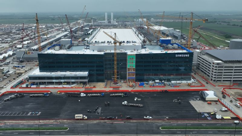
The projected pace of development of the semiconductor industry implies that construction of 18 new semiconductor production facilities will begin around the world this year. Of these, only three will work with silicon wafers of a standard size of 200 mm, the rest provide for work with a standard size of 300 mm.

The bulk of the enterprises whose construction will begin this year should begin operations in the period from 2026 to 2027, as noted in the forecast of the industry association SEMI. The leaders in the number of semiconductor industry enterprises being built this year should be America and Japan, since each of the macro-regions will launch four projects. Three projects each will be launched in China and the EME region (Europe and Middle East). Taiwan will limit itself to two enterprises, the construction of which will begin this year. Southeast Asia and South Korea will be limited to one facility in each case.
Last year, 48 enterprises for the production of chips were put into operation around the world, this year another 32 enterprises will join them; they will work with a range of standard sizes of silicon wafers from 50 to 300 mm. At the end of this year, the increase in the gross volume of production of silicon wafers with chips will be 6.6%, which in monthly terms will allow reaching 33.6 million silicon wafers. The main driver of growth will be the artificial intelligence industry’s need for specialized semiconductor components. In the segment of advanced technological processes with standards no more than 7 nm, monthly processing volumes of silicon wafers will increase by 300,000 pieces (16%) per month to 2.2 million.
Mature technological processes will be stimulated by China’s desire to achieve technological sovereignty, as well as the development of the Internet of Things and the automotive segment. In the process range from 45 to 8 nm, average monthly processing volumes of silicon wafers will increase by 6% to 15 million pieces. In the segment of technological processes rougher than 50 nm, the expansion rate will be more restrained, it will not exceed 5% and will limit the monthly processing volumes of silicon wafers to 14 million pieces.
Contract chip manufacturers will increase their capacity by 10.9% at the end of the current year, ensuring the processing of a record 12.6 million silicon wafers per month. The growth rate of memory chip production volumes will slow down from 3.5 to 2.9% this year compared to the previous one. At the same time, the main driver of growth will remain HBM memory, which is necessary for computing accelerators for artificial intelligence systems. Largely due to this, the DRAM segment will increase the average monthly processing volume of silicon wafers this year by 7% to 4.5 million pieces. The 3D NAND segment will add only 5% to 3.7 million silicon wafers per month. If now in general there are more than 1,500 enterprises and production lines for the production of chips in the world, then after 2024 about 180 enterprises and lines will be put into operation, provided that manufacturers do not abandon their plans.