At the end of July, AMD will release two series of processors – desktop Ryzen 9000 (Granite Ridge) and mobile Ryzen AI 300 (Strix Point) – based on the latest Zen 5 architecture. The HardwareLuxx.de portal has found out the missing details about these processors. In particular, the dimensions of the crystals of these chips and the number of transistors used in them became known.
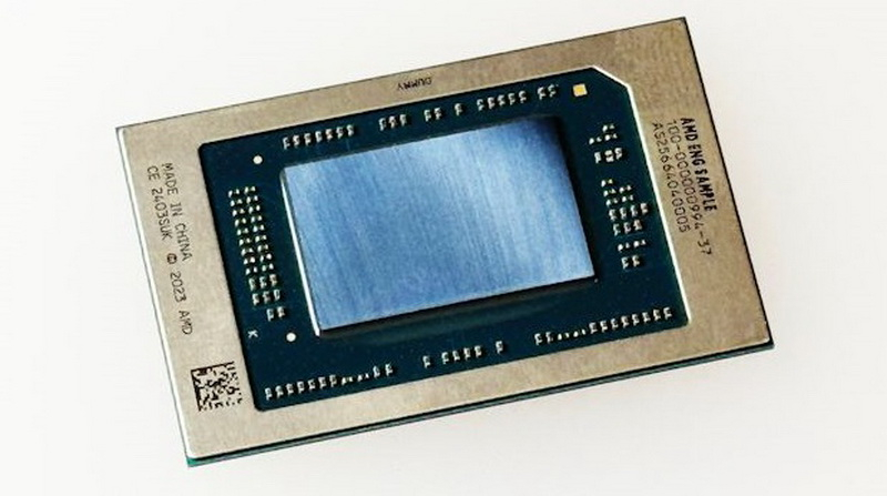
Image Source: AMD
Ryzen AI 300 (Strix Point) processors are built on a monolithic chip, which is manufactured using TSMC’s 4nm N4P process. This is a slightly improved version of the N4 process technology, on the basis of which AMD Phoenix and Hawk Point processors based on the Zen 4 architecture are produced. The Strix Point die area is 232.5 mm2. Thus, it is significantly larger than the Hawk Point and Phoenix crystals with an area of 178 mm2.
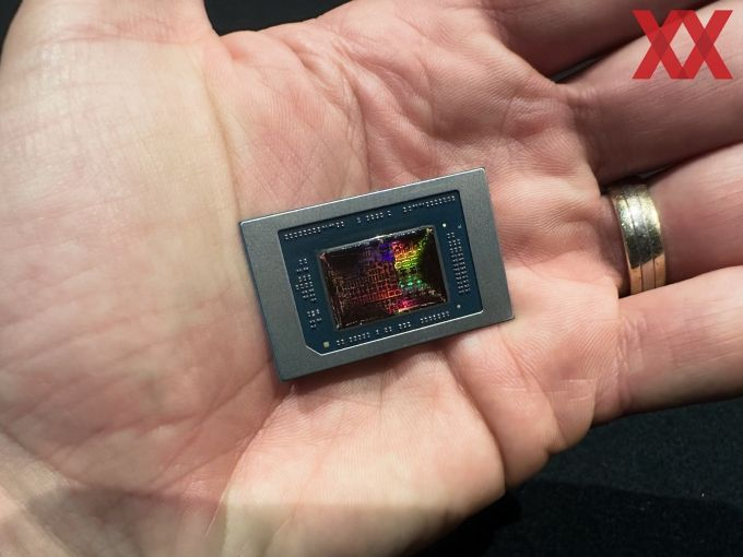
Image source: HardwareLuxx.de
The increased area of the Strix Point crystal is explained by the increased number of execution units of the integrated Radeon 800M graphics on the new RDNA 3.5 architecture from 8 to 12 for the Ryzen AI 9 365 model and from 12 to 16 for the Ryzen AI 9 HX 370. Also, the area of the new crystal has become larger due to L3 cache increased to 24 MB and in general due to larger Zen 5 and Zen 5c cores.
The Ryzen 9000 (Granite Ridge) desktop processors use a chiplet design similar to the Ryzen 7000 (Raphael). AMD has confirmed that the new processors use Raphael’s I/O die (cIOD), manufactured using the same 6nm process. The area of this crystal has not changed and is 122 mm2. It contains 3.4 billion transistors. For comparison, the cIOD processors Ryzen 5000 (Vermeer) and Ryzen 3000 (Matisse) were manufactured using Global Foundries’ 12nm process technology and had an area of 125 mm2, but contained significantly fewer transistors – 2.09 billion. A key factor in the increase in cIOD die area there was a built-in iGPU unit with two execution units.
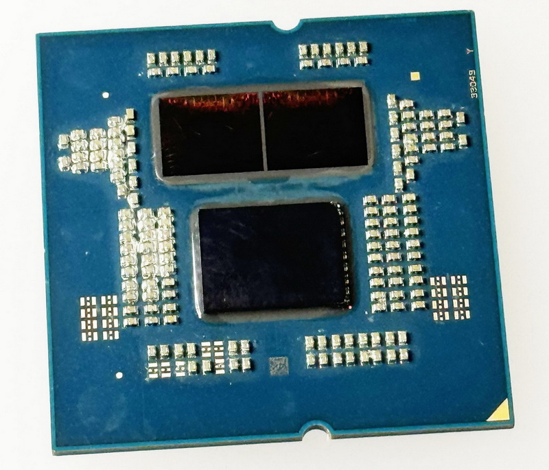
Ryzen 9000 processors use a new CCD die with eight processing cores, called Eldora. According to HardwareLuxx.de, it is manufactured on the same 4nm N4P process as Strix Point processor dies. However, according to other sources, these chips may be manufactured using the even more advanced N4X process technology, which works better at high clock speeds.
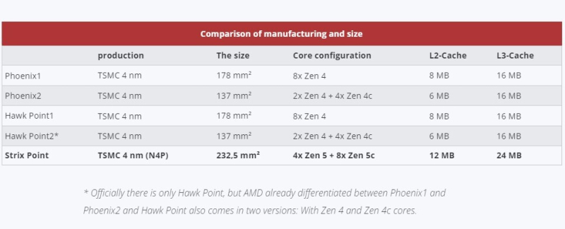
Image source: HardwareLuxx.de
The CCD die of the Ryzen 9000 processors contains 8.315 billion transistors, which is a significant increase compared to the 6.5 billion transistors in the eight-core CCD Durango die of the Ryzen 7000 chips based on the Zen 4 architecture. It is noteworthy that despite the 28% increase in the number of transistors, The CCD area of the Eldora based on Zen 5 is 0.5% smaller than the CCD area of the Durango based on Zen 4 – 70.6 mm2 versus 71 mm2. Let us remind you that CCD Durango on Zen 4 is produced using TSMC N5 5nm process technology.
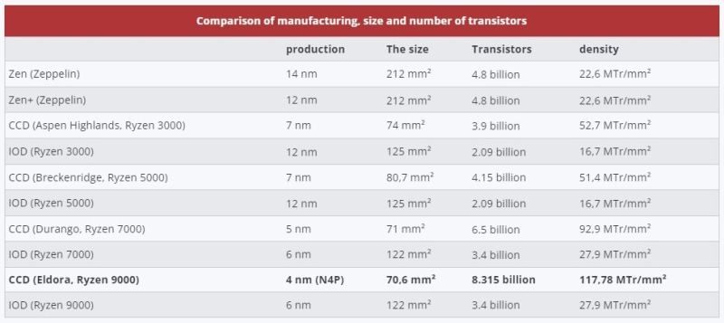
Image source: HardwareLuxx.de
Thus, the total number of transistors in the flagship 16-core Ryzen 9 9950X processor with two CCD chiplets is 20.03 billion. In turn, the Ryzen 7 9700X with one CCD contains 11.715 billion transistors.