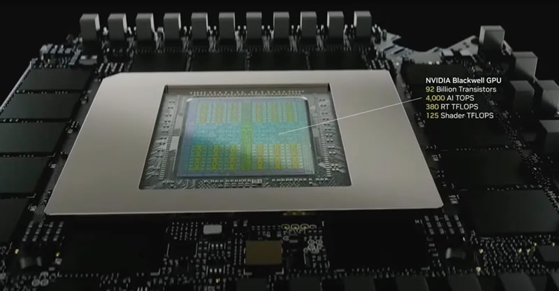
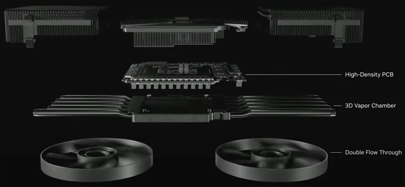
Nvidia unveiled the GeForce RTX 5090 Founders Edition at CES 2025, making it its most powerful consumer GPU to date. However, along with impressive performance, the device turned out to be one of the most power-hungry GPUs in history. To ensure stable operation at a power consumption of 575 W, the company created a three-part PCB design.

Image source: NVIDIA

Image source: NVIDIA
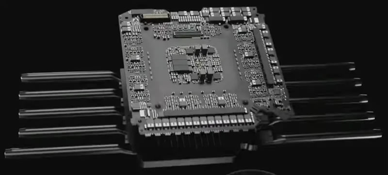
The GeForce RTX 5090 features a new 12V-2×6 connector that supports up to 600W of power at 12V to efficiently power the GPU and memory for high performance. Despite this, the main board lacks the usual connectors for displays, fans and PCIe. Presumably, this video card has two more boards that have not yet been shown, and the reasons for separating video outputs, PCIe and fan connectors from the main PCB remain a matter of speculation today.

Image source: NVIDIA
Perhaps each PCB was designed for a specific purpose, allowing for better signal routing and efficient use of space. Also, separating the connectors can minimize electrical noise and improve power supply stability to the GPU. Alternatively, Nvidia could take a page from the GeForce 8800 GTX/Ultra and separate the display engines from the GB202 GPU to save compute space and optimize the overall graphics card design.
Either way, this could allow Nvidia to offer customers products based on the GB202 chip by mixing different external modules. For example, a GB202-based card installed in a server does not require a video connector, while some OEMs might offer their customers a different I/O configuration. Thus, a three-component printed circuit board is not a mandatory requirement for top-end Blackwell video cards, but is based on a unique design solution by Nvidia engineers.