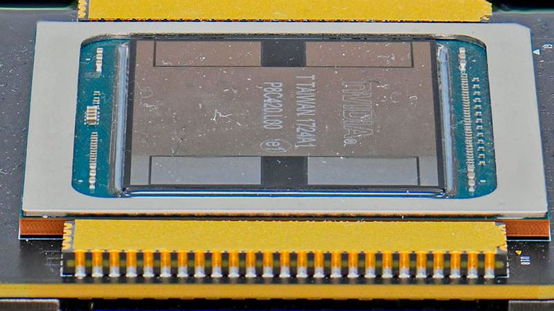
Nvidia’s explosive revenue growth amid strong demand for its compute accelerators is actually being tempered by the capabilities of its manufacturing partners, chief among them TSMC. The latter not only produces chips for Nvidia, but also packages them using the advanced CoWoS method, and the contractor’s capabilities in this area are a bottleneck for Nvidia, which it is ready to actively expand.

Image Source: TSMC
According to Commercial Times, TSMC is rapidly expanding its production capacity for testing and packaging chips using the CoWoS method in Taiwan. The Tainan LCD panel manufacturing facility it bought from Innolux will be converted to chip testing and packaging by the end of next year, and TSMC’s total capacity in this area will triple to 90,000 silicon wafers per month by the end of 2026, according to Taiwanese sources.
TSMC’s core plant in Taichung will be operational in the first half of next year, and the company is also building two plants in other areas of the island. This year, analysts estimate that TSMC was able to package and test chips using the CoWoS method at the equivalent of 35,000 silicon wafers per month. Revenue from this type of service reached 7–9% of the total. By the end of next year, capacity will double to 70,000 wafers per month, and the revenue share will exceed 10%. Finally, by the end of 2026, TSMC will be able to package the equivalent of 90,000 silicon wafers every month using the CoWoS method.
In total, from 2022 to 2026, the company’s productivity in this area will increase annually by an average of 50%, and the process will continue after 2026. The Tainan facility alone could theoretically process 50,000 silicon wafers per month. Most likely, it will eventually be only partially loaded with specialized orders, and the remaining capacity will be allocated to work with CPO and FoPLP packaging methods.