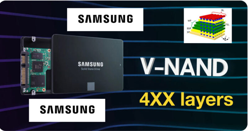
It has become known about the upcoming report by Samsung engineers at the IEEE International Solid-State Circuits Conference 2025. This will happen on February 19. Experts will talk about the future 400-layer 3D NAND memory, which no manufacturer in the world has yet.

Image source: blocksandfiles.com
According to the document, future Samsung memory will have more than 400 working layers. Crystals with separate sets of layers will be bonded to each other during the production process (WF-Bonding technology or substrate to substrate), which makes it possible to simplify the production of multilayer memory chips.
Today, memory with the highest number of layers is produced in bulk or in sample form by SK Hynix (321 layers), Samsung (286), Micron (276), Western Digital and Kioxia (218) and SK Hynix Solidigm (192). At the same time, Western Digital, Kioxia and YMTC are developing 300-layer memory, which will be presented in the coming year. The main fight for the championship flared up between SK Hynix and Samsung, which are ready to storm the frontiers of memory with 400 layers or more.
The 400-layer Samsung chip expected to be presented will have a volume of 1 Tbit with a density of 28 Gbit/mm2. Three bits of data will be written to each cell. The declared transfer speed for each contact will reach 5.6 Gbit/s, which is 75% more when compared with current 9th generation Samsung memory chips (400-layer memory will belong to the 10th generation V-NAND Samsung). Obviously, such memory is suitable for making SSDs with PCIe 5.0 and PCIe 6.0 buses.
Samsung’s denser memory could push manufacturers to release 256 TB and even 512 TB SSDs. Perhaps it will be in a year or two. Let’s wait for the February report and clearer positions of Samsung management regarding the production of new memory.