Scientists from the USA have figured out how to significantly simplify the production of microcircuits with nanometer-sized elements. Currently, chip production mainly uses masks, etching and multi-step processing with numerous rejections. Researchers have proposed a casting mold that is filled with liquid metal. The technology has shown a low level of defects and high controllability of the characteristics of cast diodes and transistors.

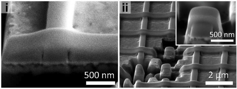
An example of cross casting. Image source: Julia Chang/NC State University
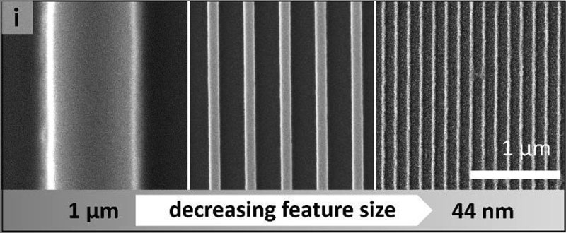
The method proposed by scientists from North Carolina State University does not reach the technological standards of modern chips. While TSMC is storming the bastion of technological processes with standards up to 2 nm, researchers demonstrate the minimum width of a wire cast from liquid metal in the region of 44 nm, and the maximum – about 1000 nm. In this contrast, it may seem that new technology has no place in the modern world. But that’s not true. Casting depends on the scale of the mold and demonstrates the dizzying simplicity of chip production, which can be used in a variety of applications.
However, we are not really talking about casting, although the production process using liquid metals is basically the same. For their work, scientists used the so-called Fields metal – a low-melting alloy of indium, bismuth and tin. The metal is placed next to the mold and allowed to oxidize—to form an oxide film on its surface. A liquid containing ligands, substances (molecules) that bind to the metal ions in the oxide, is then applied to the oxide. And this liquid with ligands and ions associated with them is launched into a form – an imprint of the future chip.

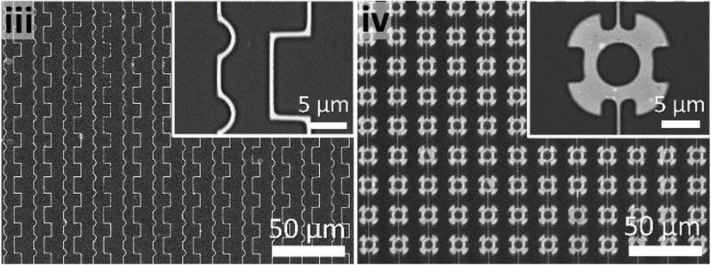
The shape options are amazing in variety and precision
Under the influence of capillary effect, the liquid penetrates into the mold. After filling the form, the composition is allowed to stand so that the liquid from the solution evaporates. This allows the mold to then be removed without damaging the casting. Finally, the casting is slowly heated to 600°C and held for an hour, which hardens the design. In parallel, the ligand composition is destroyed with the release of oxygen and carbon. Oxygen immediately binds to metal ions and forms oxides with them, which have the properties of semiconductors – the result is blanks for diodes and transistors. Burning carbon forms a graphene coating on nanowires and elements, protecting them from oxidation and improving conductive properties.

Width range of conductors in casting production
Scientists have shown that the proposed technology makes it possible to create elements that are sensitive both to light—this is ready-made photonics—and to electric current—this is electronics. There is much less defects in such production, and the speed of chip production is much higher than in modern semiconductor factories.