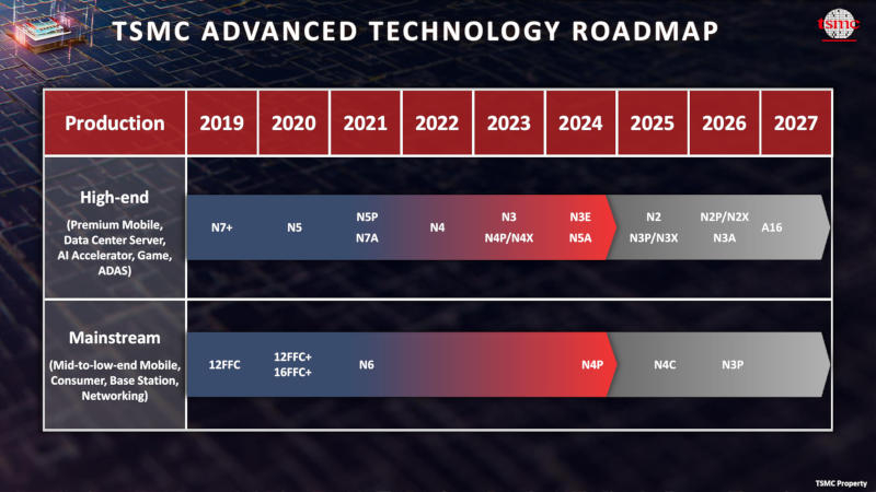
TSMC’s plans for the next couple of years remain largely unchanged – by the end of 2025 the company is preparing to launch mass production of chips using 2 nm technology, and at the end of 2026 the A16 technology (1.6 nm class) will be ready, the manufacturer said at the Open Innovation Platform conference ( OIP) 2024 in Amsterdam.

Image Source: TSMC
TSMC presented a roadmap at its own event in the Netherlands, which clearly shows its plans for introducing new solutions. N2 technology is planned to be deployed at the end of 2025 – it will be the first in the 2nm class; a year later it will be followed by improved versions N2P and N2X, after which it will be the A16’s turn. The last three are expected by the end of 2026, the company specified. No other details were provided because a contract manufacturer cannot announce products in advance for its largest customers.
Technically, N2, N2P, N2X and A16 have a lot in common – they are all based on gate-all-around (GAA) transistors. The N2 series uses Super-High-Performance Metal-Insulator-Metal (SHPMIM) capacitors to help reduce transistor resistance and thereby improve performance; and in the A16, power is supplied from the reverse side (Backside Power Delivery Network, BSPDN), which provides even higher performance. But the latter solution also has a drawback – additional heat generation, which has to be taken into account.
Thus, chips based on A16 technology with BSPDN in its current implementation are most suitable for artificial intelligence accelerators that will be used in data centers. N2P offers performance gains over the base N2 without the added complexity – a technology best suited for mobile processors and entry-level PC chips. Finally, N2X means increased performance and higher voltages – this solution is optimal for high-performance central processing units.