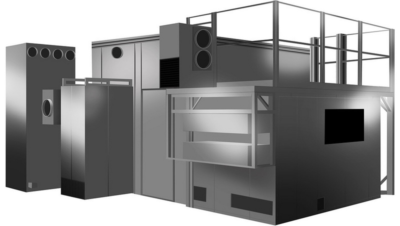
Nikon is developing a digital maskless lithography system with one-micron resolution and high throughput to produce advanced substrates for advanced chips. We are talking about substrates made of glass and other materials, which will become the basis for large and complex chips from many microcircuits. The product is planned to be released in fiscal year 2026.

Image source: Nikon
According to Nikon, the rapid adoption of artificial intelligence (AI) technology is driving demand for integrated circuits (ICs) for data centers. Despite the miniaturization of wiring circuits, the size of finished microcircuits is increasing, including due to the transition to a chiplet layout, when many microcircuits are assembled on one substrate. According to Nikon, this will lead to increased demand from chip manufacturers for a new type of packaging that uses glass and other materials suitable for producing larger chips.
The production of this type of packaging requires lithographic equipment that combines high resolution and a large exposure area. To meet these needs, Nikon is developing digital imaging equipment that combines the high-resolution semiconductor lithography technologies that the company has refined over many decades with the high throughput made possible by the development of FPD multi-lithography technologies.
The digital lithography system does not involve the use of photomasks. Instead, it emits light from a source to a spatial light modulator (SLM), which maps the outline of the circuit and transfers it to the chip substrate using a projection optical system. Without the need to design or manufacture photomasks, the digital lithography system helps reduce costs and reduce product development and manufacturing time.