The next-generation Intel Core Ultra 200S desktop processors will go on sale on October 24. On this occasion, the Chinese office of Asus decided to publish a video in which it talked about motherboards based on the Intel Z890 chipset, designed for these chips. In this video, the company also spoke in detail about the architecture features of the Intel processors themselves.
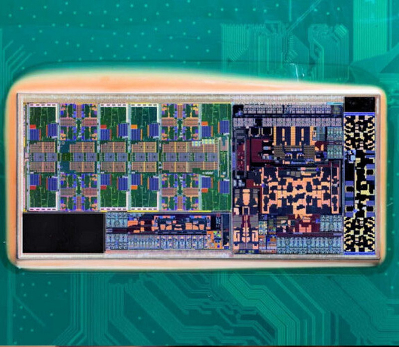
Image source: ASUS
Asus has not only removed the heat spreader cover from one of its Core Ultra 200S series processors, but also removed the top silicon layer from its four chiplets to reveal their features.
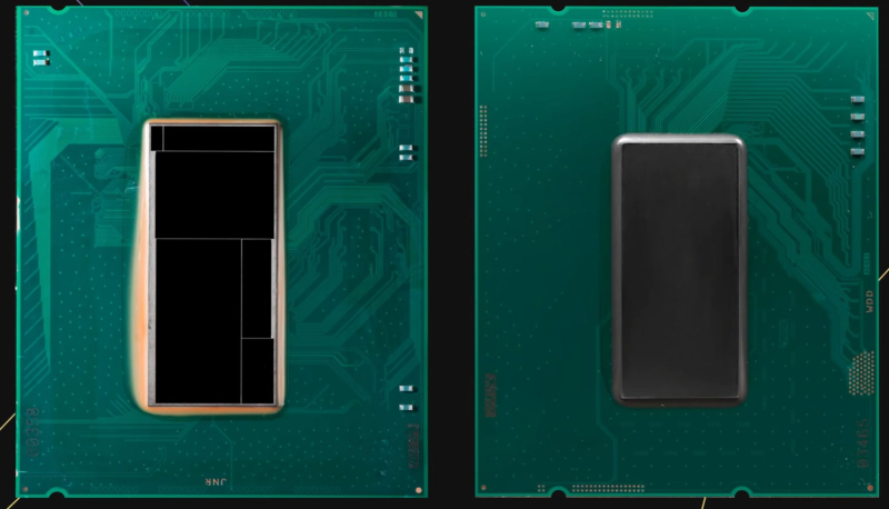
Arrow Lake-S crystals (left) and Raptor Lake-S Refresh (right)
Core Ultra 200S processors consist of four logical components (tiles or chiplets) combined on a Foveros substrate: a computing chiplet with CPU cores, a SoC die, an integrated graphics unit (iGPU), and an input/output interface die (I/O Die). The Core Ultra 200S also has two dummy chiplets, which appear as voids (black areas) in the images provided by Asus.
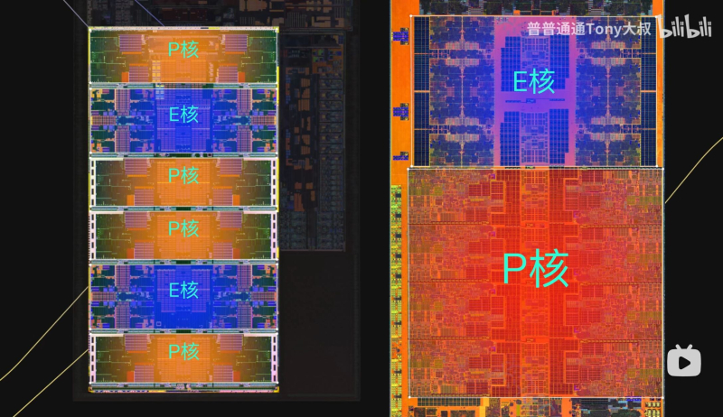
The computing chiplet with cores is manufactured on the basis of the most advanced technological process among the four crystals in the Core Ultra 200S – TSMC N3B class 3 nm. Unlike previous generations of Raptor Lake-S and Alder Lake-S processors, the new Arrow Lake-S has high-performance P-cores and energy-efficient E-cores that are not grouped together. The large and small cores of the Core Ultra 200S processors are arranged alternately: a row of P-cores is followed by a cluster of E-cores, followed by two rows of P-cores, and then another cluster of E-cores before the last row of P-cores. The end result is a configuration of eight P-cores and 16 E-cores. This core layout reduces heat concentration when the P-cores are loaded (for example, during gaming) and ensures that each E-core cluster is just one hop away from the ring bus and away from the P-core, which should improve thread migration latency. The ring bus itself, as well as 36 MB of L3 cache shared by the P and E cores, are located in the central region of the chiplet.
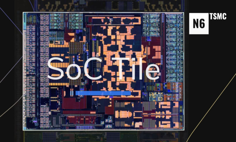
The SoC chiplet of the Core Ultra 200S processors is manufactured using the TSMC N6 6nm process technology using deep ultraviolet lithography. At both ends of the chip there are PHY circuits responsible for the operation of various input-output interfaces. On one side of the chiplet there is a PHY circuit for DDR5, on the other – for PCI Express. The SoC chiplet provides support for 16 PCIe 5.0 lanes for PCIe x16 slots on the motherboard. The SoC contains an NPU (AI accelerator) unit, which, apparently, is borrowed from the SoC of Meteor Lake processors. Its peak AI performance is 13 TOPS (trillion operations per second). The SoC also contains platform security coprocessors, as well as some iGPU elements, including a display controller (Display Engine), multimedia accelerators, etc.
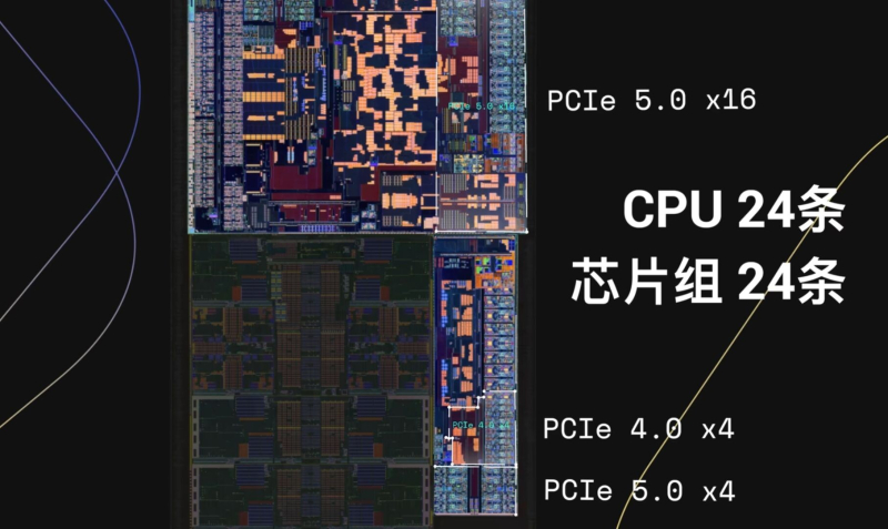
In addition to the DMI 4.0 x8 chipset bus, the I/O chiplet (also 6nm TSMC N6 process technology) provides four PCIe 5.0 and four PCIe 4.0 lanes for NVMe drives. PCIe 4.0 lanes from the I/O chiplet can be reconfigured to support Thunderbolt 4 or USB4 interfaces.
The integrated graphics unit (iGPU) chiplet of the Core Ultra 200S processors is manufactured using TSMC N5 5nm process technology. Using the same technical process (one of its versions), graphics processors of current Nvidia video cards with Ada Lovelace architecture and AMD with RDNA 3 are produced. This chiplet contains four Xe graphics cores, as well as various elements for image rendering.