The world’s largest contract semiconductor manufacturer TSMC will begin to actively use the Nvidia cuLitho computational lithography platform in production – it will help speed up product release and push the physical limits for advanced next-generation chips, Nvidia said.

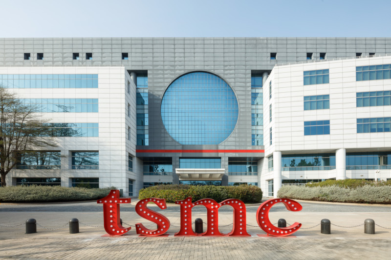
Image source: tsmc.com
Computational lithography is a critical step in chip manufacturing, necessary when moving electronic circuit designs to silicon. This process requires complex computations: electromagnetic physics, photochemistry, computational geometry, iterative optimization and distributed computing. Semiconductor manufacturing uses data centers to perform these calculations, but this stage still remains a bottleneck in bringing new processes and computer architectures to market.
Computational lithography is the most resource-intensive workload in the entire semiconductor design and manufacturing process. A typical set of masks to print a chip can take 30 million or more hours of CPU time. But 350 systems based on Nvidia H100 accelerators can replace 40,000 CPU systems—helping reduce production time, cost, space and power consumption. Nvidia has previously said that its system can handle jobs that previously took two weeks in one night. Nvidia’s cuLitho library is responsible for deploying accelerated computing in the field of computational lithography. In TSMC’s case, it will help accelerate the development of advanced semiconductor components.
Nvidia has also developed methods for applying generative artificial intelligence to the cuLitho platform, which provides an additional 2x acceleration in system performance. Generative AI helps in creating a near-perfect inverse mask that accounts for light diffraction in computational lithography; accelerated computing and AI are also responsible for optical proximity correction (OPC). Together, they make it possible to more accurately model physics and implement mathematical methods that were previously considered extremely resource-intensive. As a result, the time required to create each mask at the factory is radically reduced, which means the development cycle time for a new technological unit is also reduced.
Calculations that were previously impractical are also possible. Inverse lithography techniques have been described in the scientific literature for two decades, but their precise implementation on a full-chip scale has been largely ruled out because the computations involved are too time-consuming. Nvidia cuLitho helps solve this problem – advanced factories will be able to use it to create powerful next-generation chips.