Tech enthusiasts have conducted a full teardown of one of the Ryzen 9000 series processors (Granite Ridge) and shared highly detailed images of the CCD die (with Zen 5 cores) and cIOD (input-output) of the new processors.
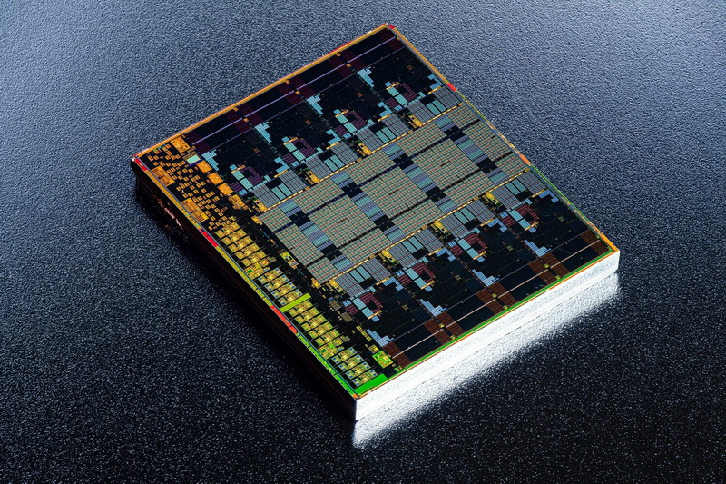
Image source: X / @FritzchensFritz
The packaging of the new chips is similar to the packaging of the predecessors of the Ryzen 7000 (Raphael). Depending on the model, the chip may contain one or two eight-core CCD chiplets, as well as one input-output die (cIOD), located in the central part of the processor board. The new Ryzen 9000 borrowed the cIOD crystal from its predecessors. Thus, AMD was able to reduce the cost of developing new chips. CCD crystals with Zen 5 cores are manufactured using TSMC N4P 4nm process technology.
The cores in the Granite Ridge CCD processors are located closer together than in the Raphael Zen 4 CCD processors. Each Granite Ridge CCD contains 8 full-size Zen 5 cores, each of which has 1 MB of L2 cache. In the central part of the CCD there is 32 MB of L3 cache memory, distributed between the cores. Other CCD components are the SMU (System Management Unit) control controller and the physical implementation of the Infinity Fabric over Package (IFoP) bus, which is needed to connect the CCD and cIOD chiplets.
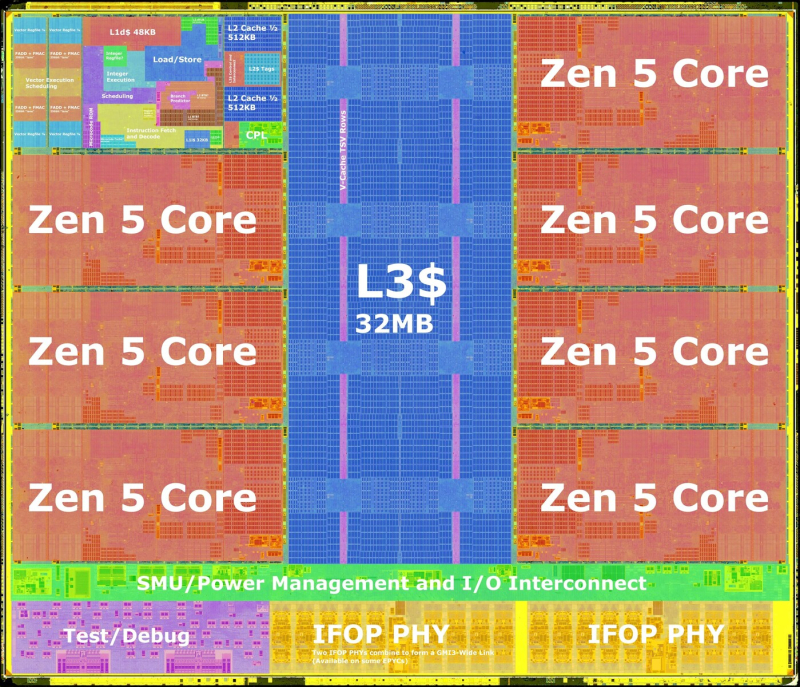
CCD unit with Zen 5 cores of Ryzen 9000 processors
Each Zen 5 core is larger than Zen 4 (manufactured using TSMC N5 process technology) due to the use of an FPU unit with native support for 512-bit data for the AVX-512. The Vector Engine is located at the very edge of the core. This makes sense since the FPU is the hottest component of the CPU core. On the other edge of the core, closer to the shared L3 cache, there are two 512 KB L2 cache blocks. AMD has doubled the bandwidth and associativity of this cache compared to Zen 4.
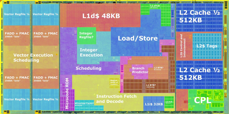
Zen 5 core diagram
The central region of Zen 5 contains 32 KB of L1I cache, 48 KB of L1D cache, Integer Execution Engine, and the input part of the processor pipeline with an Instruction Fetch & Decode unit and a prediction unit. branches (Branch Prediction Unit), micro-operations cache and scheduler (Scheduler).
The L3 cache in the central part of the 32 MB CCD die has rows of TSVs (through-silicon vias) that serve as the basis for potential “gluing” with an additional 3D V-Cache cache die. The 64 MB 3D V-Cache die can be connected directly to the internal CCD ring bus using these TSVs.
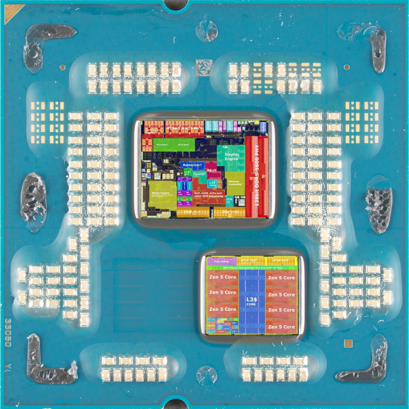
The cIOD crystal in the new processors is produced using the TSMC N6 6nm process technology. Approximately 1/3 of its area is occupied by the built-in iGPU unit and its adjacent components, such as the multimedia engine and display engine.
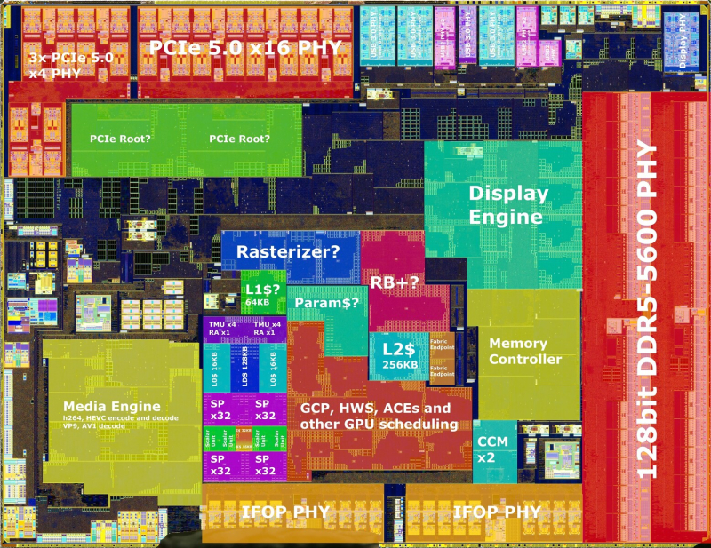
CIOD block
The iGPU, as before, is based on the RDNA 2 graphics architecture and is equipped with only one group of workgroup processors (WGP) with two execution units (CU) or 128 stream processors. Other key components of the cIOD are the PCIe Gen 5 interface with support for 28 lanes, two IFoP interfaces for interconnection with CCD core blocks, a fairly large SoC I/O with support for USB 3.x and other types of interfaces, as well as one of the most important parts of the processor – DDR5 memory controller with a dual-channel (with four subchannels) interface.