Canon has sent the first sample of its nanoprint lithography machine to a US research consortium, a major step towards commercialization of this innovative chip manufacturing method. The new technology significantly reduces costs and energy consumption. The formation of electronic circuit elements occurs due to deformation of the coating with a stamp followed by etching.
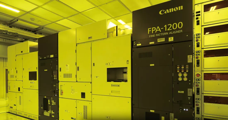
Image source: Canon
Traditional semiconductor manufacturing is done by photolithography (DUV or EUV), in which a photosensitive polymer film (photoresist) is illuminated through a photomask with a given pattern, and then the exposed areas are removed by etching.
In nanoprinting lithography, an image is formed due to the mechanical deformation of a polymer coating by a mold. Using nanoprinting lithography, it is possible to obtain nanostructures with a size of less than 10 nm over fairly large areas, which is inaccessible to all other lithography methods.
The advantage of nanoprinted lithography over photolithography is the ability to reduce production costs and energy consumption. While conventional photolithography equipment requires arrays of lenses or mirrors, Canon’s machines have a simpler design and consume ten times less power.
Nanoprinted lithography is also excellent for forming complex 3D designs using a single die, a process that is virtually impossible with photolithography.
Despite the potential of the new technology, there are still obstacles to its commercial use, the most significant of which are defects and defects caused by the ingress of tiny dust particles.
The delivery of Canon’s first full-featured testing machine to the Texas Institute of Electronics (TIE), backed by leading semiconductor manufacturers, hints at a major change brewing in chip manufacturing. Canon Deputy General Manager for Optical Products Kazunori Iwamoto announced plans to ship 10 to 20 machines per year over the next three to five years.
The Texas Institute of Electronics (TIE) is a consortium supported by the University of Texas at Austin. It includes semiconductor industry heavyweights such as Intel, NXP and Samsung, as well as numerous government agencies and academic institutions.