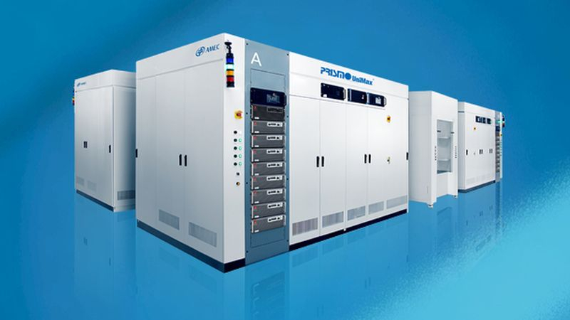
The initial reaction of the TrendForce resource to the appearance in the government catalog of Chinese equipment for the production of chips with an interlayer overlap accuracy of 8 nm was superficial, as the same source now makes clear. The equipment promoted by Chinese officials is suitable for the production of chips using 55-nm technology or cruder ones, and is far from being comparable to foreign samples that allow the production of 8-nm chips.

AMEC
A deeper analysis of Chinese documents, as explained in a new TrendForce publication, reveals that some suppliers in the local market are offering lithography equipment made in China that allows working with deep ultraviolet radiation (DUV). One of the samples is equipped with a krypton laser source, and the other with an argon source. The first is capable of working with silicon wafers of a standard size of 300 mm at a laser wavelength of 248 nm and a resolution of no more than 110 nm, ensuring an interlayer alignment accuracy of no more than 25 nm. The second Chinese-made lithography system is capable of processing silicon wafers of size 300 mm at a laser wavelength of 193 nm and a resolution of no more than 65 nm, which is combined with the notorious interlayer alignment accuracy of no more than 8 nm.
As the source explains, even such parameters, advanced for Chinese equipment, will not be enough to produce chips according to 8-nm standards. The accuracy of interlayer alignment in the production of 8 nm chips should be within the range of 2 to 3 nm, and for the described Chinese sample it is three or even four times worse. In particular, for the production of chips using 10-nm class technological processes, an interlayer alignment accuracy of no more than 3 nm is required, and for 7-nm chips – no more than 2 nm.
If we talk about resolution, then for the advanced technological processes described it should be no higher than 38 nm, and the most advanced Chinese sample has a resolution at the level of 65 nm technological process. With such equipment, according to TrendForce representatives, it is difficult to establish economically viable production of even 40 nm chips. A reasonable limit in practice corresponds to 55 nm, and even then you will have to use complex equipment that does not guarantee an acceptable level of defects.
SMIC manages to produce 7nm chips for Huawei, but for this it uses multiple exposures, which ensures a fairly high level of defects, as well as DUV-class equipment from the Netherlands ASML, imported even before the current sanctions were introduced by the United States and the Netherlands. Chinese-made equipment cannot yet provide such capabilities, and has not even come close enough to them.