Multi-layer and multi-level NAND cells are truly a masterpiece of semiconductor technology. However, with their further miniaturization from the level achieved to date, things are not at all simple: for fundamental physical reasons, even reducing the size of nanocapacitors, which serve as basic elements for data storage, is an incredibly difficult task. Increasing the number of data bits stored in one cell – moving from the most common three- and four-bit memory chips (TLC and QLC) to five-bit (PLC) and more – is also a strategically dead-end option: the likelihood of errors during operations with such cells increases noticeably, and their durability (the number of rewrite cycles after which the nanocapacitor simply fails) is dramatically reduced.
Suffice it to say that SSD customers for cloud AI servers – and it is this relatively narrow segment of the global drive market that has recently shown outstanding growth, amounting to tens of percent quarter by quarter – prefer, according to TrendForce experts, not five-, not four-. , but just three-level (TLC) devices with a capacity of 4-8 TB, since these are the ones today that demonstrate the optimal ratio of the three most important parameters for business. Namely – high capacity; performance sufficient for AI tasks under high load; and at the same time durability, which certainly makes it possible to pay for their installation in commercial systems. In other words, the development of NAND technologies from the point of view of hyperscalers, which provide cloud access to entrprise-level AI models, has essentially hit the “glass ceiling” of justification for investments – it’s time to look for something new to replace them. Something with the same significant development potential that the same semiconductor memory had a dozen or two years ago.
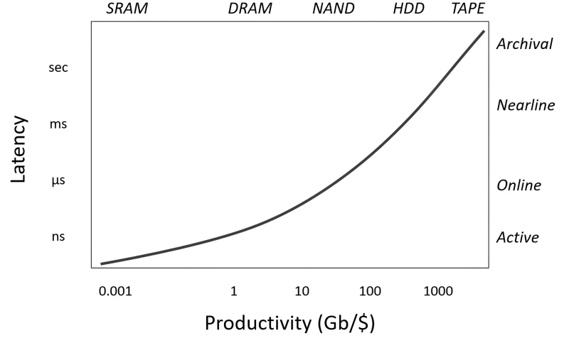
Varieties of physical implementations of computer memory (SRAM – operational, DRAM and then – permanent) in the coordinates “availability in GB / dollar.” — “access delays (on a logarithmic scale)”, as well as their applicability for different types of data storage: archival, deferred access, online, always active (source: IMEC)
It is expected that by 2029, 3D NAND chips will be able to provide data recording densities of up to 70 Gbit/mm². This in itself is a very impressive value – even if we leave aside the question of what delays computer systems of the near future will face when accessing such information-rich semiconductor structures. But you will have to contact them – especially during the training of new ones; much more sophisticated artificial intelligence models than those available today. The growth dynamics of their appetites are impressive: for training GPT-3, for example, a data set of 570 GB was used (the volume of compressed text is indicated – only text, without images and videos, since this is not a multimodal model – and even after filtering the original, much larger array), which generated 400 billion tokens. According to expert estimates, more than 280 TB of filtered data, converted into over 70 trillion tokens, have already been used to train the upcoming GPT-5 (presumably it will be presented to the public in November-December 2024, after the American elections). The increase in the volume of information required for training a model by almost three decimal orders in just about a couple of years is staggering, and if such rates are at least partially maintained, and the current generative AI is not replaced by some less resource-hungry way of organizing machine learning for To solve the same problems, the global IT industry will need a lot of capacious storage devices. Perhaps a considerable share of them will turn out to be liquid-based in a relatively short time – and within this direction that has just begun to develop, they have already managed toSeveral competing technologies take shape.
⇡#Nanosize matters
In 2022, researchers from the Belgian IMEC (Interuniversity Microelectronics Center) proposed two approaches to organizing liquid permanent memory: colloidal and electrolytic, each of which in the future opens up the possibility of creating drives with a data recording density of up to 1 Tbit/mm². Considering how much the density growth rates of increasingly “multi-story” NAND chips appearing in recent years have decreased, the development of liquid-based storage (LBS) seems more than attractive – even taking into account the considerable investments required for this. According to the authors of this idea, liquid memory may begin to appear in the form of serial data storage from the early 2030s, and by that time, in terms of access speed, it will be able to occupy an intermediate position between HDD and tape cassettes. 3D NAND in 5-6 years will continue to remain unsurpassed in terms of response speed, however, in such tasks as creating backup copies with the ability to quickly search and retrieve data, as well as storage – not archival, but, as they say, at hand; nearline – multimedia collections and other voluminous files LBS has every chance of displacing the hard drives that are familiar today. Especially considering the fact that they also seem to be reaching a plateau in the growth of the density of information stored on magnetic plates.

Three approaches to organizing computer memory: a) semiconductor – combining access devices with storage cells, b) magnetic – unallocated storage medium with a moving access device, c) liquid – with a volumetric storage medium and stationary access devices (source: IMEC)
Let’s remember why semiconductor memory, be it DRAM or NAND, is extremely difficult to miniaturize beyond a certain scale. Each cell of such a data storage, single- or multi-level, consists of at least one actual storage element – storing an electric charge – as well as an access device to this element; a conditional switch, which is played by a diode or transistor. Through a switch, the storage element is connected to electrical buses, through which commands to read/write/reset cells are received. Although the storage element can theoretically be miniaturized down to the molecular scale, especially if we move from capacitors to monomolecular magnets, the switches and data buses in a semiconductor device will inevitably continue to remain relatively macroscopic objects – the minimum characteristic size of which is determined by the characteristics of the technological process that is used to manufacture a given chip.
In the case of HDDs and especially tape cassettes, the organization of data storage is fundamentally different: there is either one access device or is represented by a limited number of read/write heads, each of which serves its own area of the medium – a magnetic disk or tape, respectively. The media most often represents an unpatterned medium – although recently, with the development of HAMR/MAMR technologies, and in the future BPM, talk is beginning to be about precisely targeting heads almost at individual magnetic domains on the surface of disks. The use of an unpartitioned medium reduces the cost of magnetic data storage technologies compared to semiconductor ones – but at the expense of an obvious increase in the access time to each individual bit, as well as the amount of energy required for each write/read act (at least due to the need to physically move the heads over the storage medium ). But reducing the geometric sizes of these bits is much more effective than in the case of the same NAND.
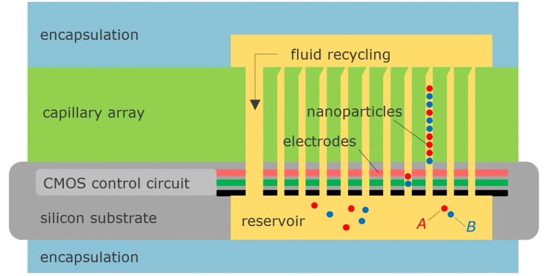
Schematic diagram of the organization of colloidal memory cells; see text for explanation (source: IMEC)
⇡#Give me the colloid!
The approach to data storage proposed by IMEC researchers is, in a sense, intermediate between classical semiconductor and magnetic. There is also a volumetric (as in 3D NAND, for example) storage medium – but the data access devices are located in a dense flat array, each element of which controls information in a column of matter – the “well” – directly below it (or above it; there is no fundamental difference here no, because in such narrow wells capillary phenomena are more significant than the effects of gravity). Thus, compared to semiconductor memory, the number of switches per bit of stored data is significantly reduced; which means that the possibilities for miniaturizing such a storage device as a whole are becoming wider. Considering the “data well” not abstractly, but quite literally, it is not difficult to repeat the mental path of IMEC engineers to the concept of colloidal memory – when vertical recesses in the physical base of the drive are filled with a colloidal system, i.e. one in which they are contained heterogeneously, without mixing or interconverting , at least two phases in different states of aggregation. Most often this is a liquid medium (in this case, distilled water) and a solid filler. The latter is represented by nanoparticles of two types, some of which encode ones, others – zeros, and their physical dimensions are such that they fit freely into the trunk of the data well, without effort, but strictly one by one.
Thus, a sequence of symbols written into a base cell, a conventional machine word, will simply be a sequence of particles with different properties – the main thing is to select them so as to confidently distinguish between “zeros” and “ones” when reading information and freely manipulate them when writing . For these operations, IMEC proposes to use conventional semiconductor CMOS structures, which means that the types of particles—data carriers in colloidal memory—should differ from one another, for example, in the magnitude of the electric charge. There are no big problems with reading: “pulling” charged nanoparticles one at a time from a certain well-capillary and fixing them at the exit from its barrel, “zero” has now returned to the common reservoir, or “one” is a simple matter. Another issue is recording data: catching a particle with the required amount of charge in a reservoir and placing it in a strictly defined well is definitely an engineering task with an asterisk.
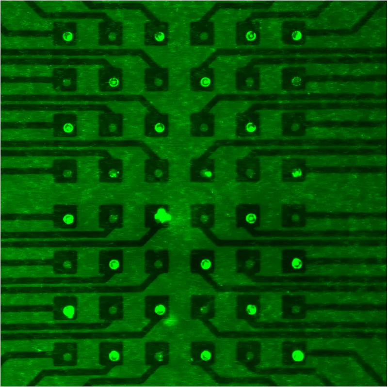
The bright dots are fluorescent polystyrene nanoparticles that enter (the difference in brightness corresponds to the depth of immersion) into the square wells of the colloidal storage prototype during the recording process (source: IMEC)
Using electrically charged particles in this case would be reckless: in a common reservoir it will not be possible to avoid parasitic attraction/repulsion between them, which will complicate the path of colloidal “bits” to selective placement in the desired capillaries. The researchers relied on the phenomenon of frequency-dependent dielectrophoresis: thanks to it, it is possible to separate particles in a liquid medium under the influence of an external electric field – themselves neutral, but reacting differently to different electromagnetic frequencies. Here, of course, there is still a lot of not only practical, but also theoretical work: for example, it will be necessary to develop an effective recording protocol that is both fast enough and guarantees against an unacceptable number of errors. The general principle is already clear: let’s say, when an external field with a conditional frequency of “0” is applied, “zero” particles will flow from the reservoir into all well-capillaries of the storage device, and the task of the CMOS controller will be to block the necks of those capillaries into which the next There is no need to write down “zero”. One way or another, IMEC has already confirmed the functionality of the colloidal storage device experimentally on the micron size scale; now the only question is finding funds and allocating engineering resources to scale it up to nanometer sizes of the main working elements.
⇡#And the electrolyte won’t hurt
Another type of liquid storage proposed by Belgian researchers is electrolytic. Electrolysis, we recall, is the process of formation of chemical products on electrodes (which are in contact with a medium with ionic conductivity) when an electric current flows through a closed circuit formed by such contact. In this case, the role of the medium is played by a solution – in water or another suitable liquid – of two metal ions, the readiness of each of which to deposit on the electrode directly depends on the magnitude of the potential applied to the circuit. The drive itself, also, as in the case of colloidal memory, is a reservoir for liquid with an array of capillaries, but only here at the bottom of each well there is an individual control electrode (controlled, again, by a CMOS circuit), and on the opposite side of the reservoir there is a common large electrode, one for the entire array.
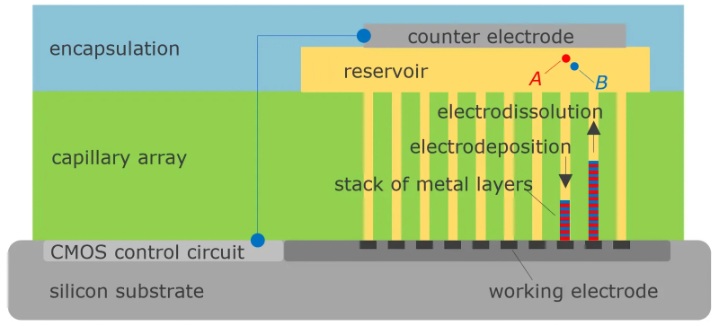
The operating principle of electrolytic liquid memory: the arrows show the process of ion deposition (electrodeposition) and the reverse process of returning metal layers previously accumulated in the capillary into solution (electrodissolution) (source: IMEC)
The principle of operation of an electrolytic storage device is also quite transparent: by applying a certain potential to the control electrode in one of the capillaries, the system forces ions of either one or another metal from the solution to be deposited on it (i.e. in the barrel of the corresponding well). The data encoding method proposed in IMEC consists of using one of the metals to record information (conventionally, a layer 1 nm thick will mean “0”, 2 nm – “1”), and the second to form intermediate layers between those laid sequentially in the well “bits”. The data is read by starting electrolysis in the opposite direction – calculating the change in the potential of each capillary as the previously recorded information flows out (literally) from it. Here, too, many technical problems will have to be solved – for example, the interpenetration of two metals at the interface between them may turn out to be deep enough (remember, we are talking about layers 1-2 nm thick) to then lead to reading errors. And yet, in the IMEC experiment, it was possible – using, however, arrays of millimeter and micrometer diameter capillaries for now – to achieve reliable electrolytic deposition, and then controlled dissolution (with fixation of this process at the level of control electronics, i.e. with the execution of the read operation) two layers of CoNi ions interspersed with three layers of Cu ions. Moreover, the smaller the cross-section of the well, the higher the writing and reading speeds turned out to be.
Belgian researchers, fully aware of the complexity of the engineering tasks facing developers of liquid memory, nevertheless talk about the achievability by the early 2030s of an information recording density in drives of this kind that is prohibitive by current standards – 1 Tbit/mm², and they estimate the cost of these data storages in terms of unit occupied area as lower than that of the most advanced 3D NAND chips at that time. Technological optimism is added to this forecast by calculating the density of placement of liquid storage elements necessary to achieve the stated goals: only 40 nm between adjacent structures – be it nanocapillaries or control metal buses. Even by current microelectronic standards, these are indeed quite gentle specifications, and even more so in the expected realities of 2030. Apparently, lithographic methods will become the main ones in the production of liquid memory, since modern equipment for semiconductor manufacturing is excellent at etching nanometer-diameter holes at precisely designated positions. By the way, it is the progress in the field of 3D NAND that makes it possible to form smooth vertical wells on a silicon substrate with a height-to-diameter ratio of 200:1 and even 400:1—just about the same that will be required for serial samples of electrolytic and colloidal liquid memory, respectively.
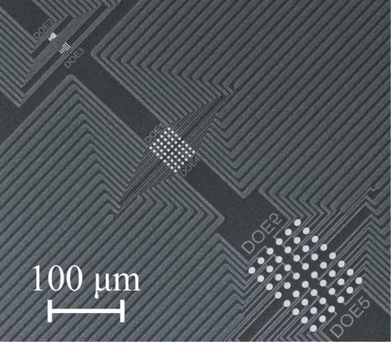
The surface of the microcircuit that served the researchers as confirmation of the concept of electrolytic memory: groups of white circles are arrays of wells with a diameter of 80-150 nm (different groups of capillaries – to assess the dependence of the speed of write/read operations on their dimensions) and a depth of 300 nm (source: IMEC)
⇡#Did you call T-1000?
The memorable “robot made of liquid metal” (more precisely, made of a metal polyalloy), with which Arnold Schwarzenegger’s character fought in the second film of the “Terminator” franchise, inevitably comes to mind in connection with the rather recent (publication dates back to the end of 2023) development of scientists from Beijing Tsinghua University – FlexRAM. As the name already implies, this is “flexible” RAM – intended primarily for equipping devices with flexible screens. At the same time, FlexRAM also contains a substance in the liquid phase: it is a gallium-based liquid metal (GLM), the melting point of which is noticeably lower than room temperature, like mercury, for example, and which, for this reason, under normal conditions remains in a liquid state.
The surface of drops of liquid metal – as, in fact, of particles of almost any solid – is subject to natural processes of oxidation and reduction, during which metal atoms either combine with oxygen (usually atmospheric: this is how rust, patina, etc. are formed) or, accordingly, lose contact with him. In the case of FlexRAM, these processes are controlled: under the influence of a low control potential, the surfaces of GLM droplets placed in the hydrogel are oxidized; The oxide film prevents the passage of electric current, thereby increasing the resistance of a given volume as a whole. The developers assigned this state to a logical unit. If the same potential is again applied to the volume, but with the opposite sign, restoration will occur – and the conductivity of this area of the medium will increase; This is how a logical zero is encoded.
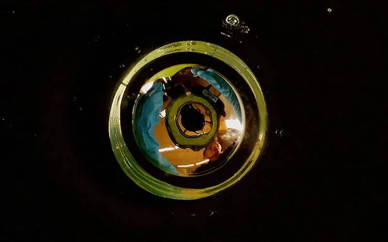
This picturesque photo captures the moment when the surface of a GLM droplet transitions from an oxidized state to a reduced state (source: Tsinghua University)
So far, the development of Chinese engineers is at a very early stage: each GLM droplet encodes one single bit of data, and the experimental setup confidently operates, writing and reading information, with only eight droplets at a time – a total of 1 byte. There is, however, an extremely important circumstance that forces researchers to predict solid prospects for FlexRAM: this memory, formally in all respects operational, is in fact capable of storing data recorded in it for quite a long time. In an oxygen-free environment, the surfaces of GLM droplets remain oxidized or reduced in the absence of external influences for quite a long time—experimenters claim 12 hours. The stability of such a simple physical and chemical system is also quite high: it has been confirmed that it can withstand at least 3.5 thousand rewrite cycles (changes in the state of the surface from oxidized to reduced and back), which corresponds to the resource reserve of cells of modern (multi-level) NAND chips.
Promising areas of application of FlexRAM – of course, after it is possible to move from the current millimeter scale to micro-, or better yet, nanometer – are called brain-machine interfaces, including implantable ones; flexible or even entirely liquid-phase computing systems; soft robotics, etc. They even talk about the similarity of oxidation/reduction processes on the surface of liquid metal droplets with hyperpolarization/depolarization of the cell membrane of a neuron – thereby implying the applicability of liquid memory for creating neuromorphic computers that closely imitate biological objects.
«Sierpinski carpet”, formed by DNA molecules during self-assembly according to an algorithm programmed by researchers (source: Wikimedia Commons)
We should not forget about another direction that has recently attracted researchers – DNA memory and, more broadly, full-fledged DNA calculations with the implementation of both data storage and logical operations on them on these well-known (at least by hearsay) macromolecules. DNA memory is good for information arrays that require only delayed access (nearline storage), as well as for long-term archival storage: under ideal conditions, without self-destructing or requiring any maintenance, it remains unchanged for decades. You don’t even have to think too much about how to encode data into DNA: this molecule was created by nature itself specifically for recording (with subsequent copying) genetic information in the form of a specific sequence of nucleotides. And the data density there is in perfect order: the entire contents of the Library of the American Congress (74 million MB as of 2021) will fit into a tangle of DNA molecules the size of a poppy seed.
Since a liquid medium is most suitable for DNA, computers (or separate data storage facilities) created using this technology will certainly also fall into the liquid category. In this area, researchers also expect many challenges – take at least the extremely low write/read speed: for example, the American MIST (Molecular Information Storage) program sets as its short-term goal to ensure the reading of 10 TB of data from an experimental DNA storage in 24 hours, spending no more than 1 thousand US dollars. Another serious challenge is not the highest reliability of data storage, especially during replication: the tendency for variability of the genetic code is built-in, one might say, at the hardware level – it is thanks to it that biological evolution occurs. In any case, liquid memory and, more broadly, liquid-based computing systems look very promising in light of the increasingly slowing pace of classical semiconductor progress.
⇡#Related materials
- Tiny capsules have been proposed for storing data on DNA – this will reduce the level of errors and protect against information loss
- Shakespeare’s “Hamlet” was encoded in DNA and showed a quick search using keywords
- IT stories: Artificial DNA – a candidate to replace silicon?