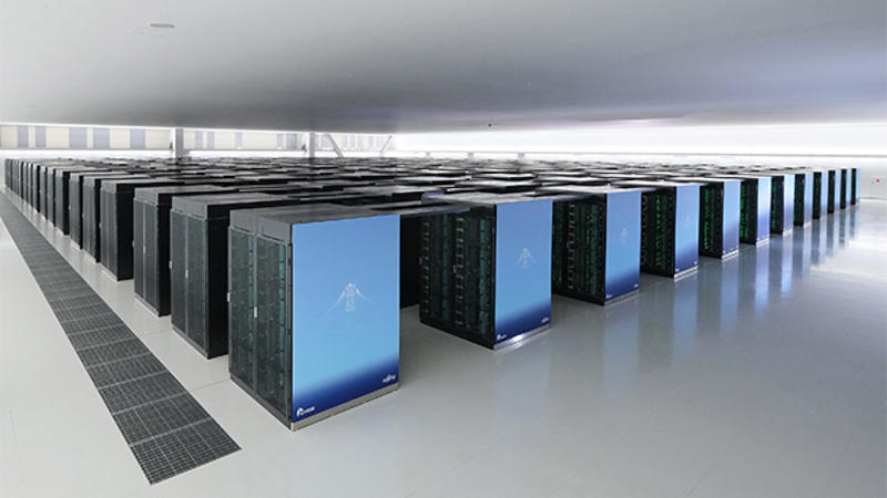
Japan’s Ministry of Education, Culture, Sports, Science and Technology (MEXT) has announced plans to build a successor to the Fugaku supercomputer, previously the fastest in the world. The Institute for Physical and Chemical Research (RIKEN) and Fujitsu will begin its development next year, Nikkei reports.
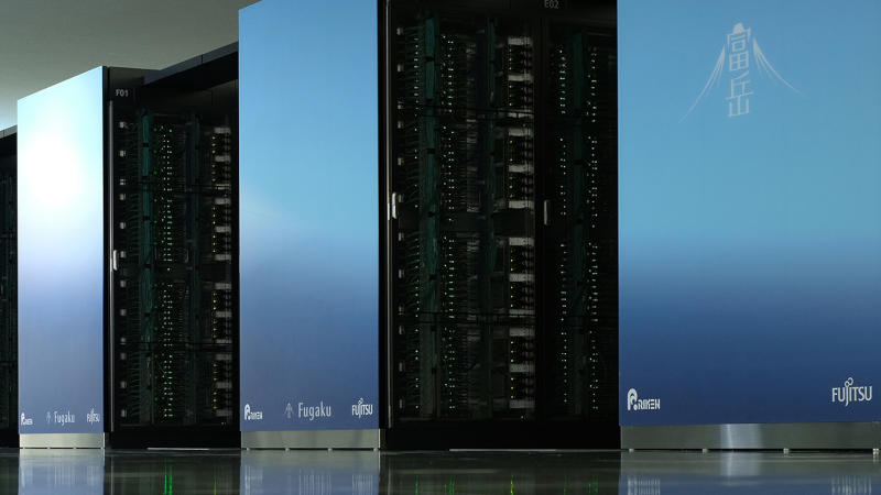
Image source: riken.jp
The new supercomputer will demonstrate performance for artificial intelligence algorithms of 50 exaflops with peak zettaflop-scale performance in selected tasks – the machine will be used to work with AI for scientific purposes. In other words, the system will be able to perform one sextillion floating point operations; zettaflops are a thousand times faster than exaflops, and if Japan builds such a system by 2030, it will truly have the most powerful supercomputer in the world.
Each compute node on the Fugaku Next supercomputer will have peak performance of several hundred teraflops for double-precision (FP64), about 50 petaflops for FP16 precision, and about 100 petaflops for 8-bit precision; HBM memory will provide a throughput of several hundred TB/s. By comparison, the Fugaku compute node delivers 3.4 teraflops of double-precision, 13.5 teraflops of half-precision (FP16), and 1.0 TB/s of memory bandwidth.
For the first year of development of the system, the ministry will allocate 4.2 billion yen ($29.05 million), and total government funding will exceed 110 billion yen ($761 million). The development will be led by RIKEN, one of Japan’s most renowned research institutes; and taking into account the fact that MEXT requires the maximum presence of Japanese technologies in the system, equipment development will be primarily carried out by Fujitsu. The MEXT documents do not indicate any specific requirements for the Fugaku Next architecture – it will probably be central processors with specialized accelerators or a combination of central and graphic processors.
If the successor to Fugaku runs on Fujitsu processors, it will receive chips that will come out after MONAKA, which have up to 150 Armv9 cores on board. We are talking about a component in a multi-chip configuration, distributed over multi-core crystals and SRAM and I/O crystals. The latter provide work with DDR5 memory, as well as PCIe 6.0 and CXL 3.0 interfaces for various accelerators and peripherals. The core dies will be produced using TSMC’s 2nm process. The successor to Fujitsu MONAKA will have a larger number of cores and more powerful interfaces – it may be manufactured using a 1 nm class process technology or even more advanced.