The largest contract manufacturers of chips are one way or another moving towards power supply on the reverse side of the chip, as it allows optimizing the chip layout and improving its performance. Samsung Electronics expects its 2nm backside power supply technology to reduce die area by 17%.
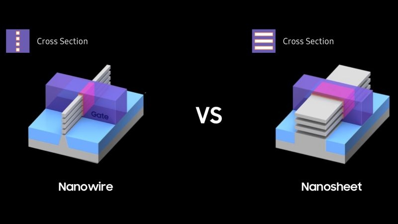
Image Source: Samsung Electronics
As TrendForce reports, citing South Korean media, the corresponding statements on Thursday were made by Lee Sungjae, vice president of the Samsung Foundry PDK Development Team, during his speech to the company’s partners. In addition to reducing the die area by 17%, the transition to power supply on the reverse side of 2nm chips will increase their performance by 8% and improve energy efficiency by 15%.
Let us recall that competing Intel plans to use similar technology in the mass production of chips using 20A technology before the end of this year; in its implementation it received the designation PowerVia. Taiwanese TSMC will implement a similar solution called Super PowerRail as part of the A16 technology in 2026. In this case, the first will use a new structure of RibbonFET transistors, and the second will introduce transistors with “nanosheets”.
Samsung’s latest technology is called MBCFET. The Korean company intends to use the second generation of transistor structure with surrounding gate (GAA) from the current half of the year, and also use it within the framework of the 2nm process being mastered later. SF3 technology itself increases chip performance by 30%, improves its energy efficiency by 50%, and also reduces die area by 35% compared to the first generation GAA. When combined with back-side power supply (BSPDN), this transistor structure will provide additional benefits.