Technological progress in the semiconductor industry, as we have noted more than once, is an expensive pleasure. According to analysts at UBS Group AG, Taiwanese TSMC will increase its capital expenditures to $32 billion by the end of this year, and will increase them even more in 2025, surpassing the $37 billion mark. Most of these amounts will be used for deployment and the commissioning of new production lines designed to produce microcircuits according to the technological standards of “2 nm” (and in the near future – “14 Å (angstrom)”, i.e. “1.4 nm”), because already now, by mid-2024, it becomes clear that the interest of the company’s potential customers in these particular production processes turned out to be higher than last year’s and earlier forecasts.
Not far behind TSMC are its main competitors in the field of VLSI production using the most advanced technological standards – South Korean Samsung Electronics and American Intel, which also intend to master mass production of 2-nm chips in 2025. And taking into account the fact that the huge sales market of mainland China (plus a number of other countries classified as unfriendly by the US Department of Commerce) for such products will most likely be closed – in the sense that companies from the PRC will not be allowed to place orders for the 2-nm products entering production ” lines, not to mention the acquisition of the corresponding chip-making equipment – the confrontation between the leaders of the global semiconductor industry promises to be truly heated.
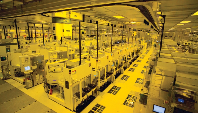
It is in such workshops, flooded with amber-yellow light (to prevent even accidental damage to the UV-sensitive photoresist), that “2nm” chips will soon be produced – to the delight of all generative AI lovers (source: TSMC)
Their clients, as well as the end consumers of IT products built on these chips, on the contrary, have something to rejoice at: it is likely that even with a fairly high cost, suppliers will have to compete with each other to keep retail prices at a level that is attractive to the wide market. This means that 2025 has every chance of becoming another year of a semiconductor breakthrough – making, for example, the notorious generative AI models even more accessible for local (and not through cloud services) execution. And at the same time, encouraging game makers to create even more exciting and fascinating games with increased system requirements. If, of course, everything goes according to everyone’s plans.
⇡#Money loves the account
Formally, there seem to be no obstacles to the implementation of these plans: ASML is regularly assembling new High-NA EUV lithography machines, ready in the future to ensure the creation of microcircuits of the “angstrom” class; The US government continues to allocate promised multibillion-dollar subsidies both for the development of its own chipmaking enterprises (Intel and Micron in the first place), and for the construction of the latest factories by TSMC, Samsung Electronics and other foreign companies in the United States. And if the world economy continued to develop along the same path – with near-zero refinancing rates of leading central banks, with American treasury securities as undoubtedly the most reliable asset, which ensured an uninterrupted flow of funds into the country’s economy and from there their targeted redistribution to the most pressing needs – surely Already this year, those same, for example, Arizona factories of TSMC and Intel, the construction of which was stimulated by the CHIPS Act adopted by the US Congress more than two years ago, would begin to produce their first products.

A device for precision selective mounting of prefabricated chiplets onto a common substrate to form a composite chip using Foveros technology (source: Intel)
However, for now, the planet’s leading chipmakers are faced with a dilemma: they need to increase investments in new technologies, but at the same time cut costs and pay off previously accumulated debts. In early August, the international agency Moody’s lowered Intel’s credit rating to BAA1 (from the previous A3), justifying this step with expectations of a deterioration in the company’s profitability indicators over the next year and a half. We are talking specifically about profit (roughly speaking, this is net revenue minus taxes and minus operating costs), which will not go to shareholders, since just in 2025-2026 Intel will have to invest a lot in the development of progressive production standards and in the construction of new factories. The situation is aggravated by the reduction in demand for the company’s products – mainly central processors – in almost all market segments: for example, despite its own problems (take, for example, the recent discovery of the Sinkclose vulnerability), AMD, according to Mercury Research, is methodically, although slowly, improving its positions in the areas of server and consumer processors.
Of course, the quarterly results that disappointed shareholders are not a death sentence at all: analysts from the same Moody’s expect that the Intel Foundry manufacturing division will be able to reach operating breakeven by 2027 – if, of course, the company as a whole establishes mass production of chips at low cost and at the same time the most advanced technical processes: both for our own design projects and as an ODM supplier for third-party customers. But this is not at all simple, given the estimated typical cost of one already mentioned High-NA EUV photolithograph of 350 million US dollars – just for this machine itself; without additional costs for its installation, adjustment and preparation for mass production. As we have noted more than once in a series of articles devoted to chipmaking technologies, each successive stage of progress in this industry costs many times more than the previous one. But while the sales market for microcircuits made according to the most advanced standards was steadily expanding, this increase in price was fully justified in economic terms – guaranteeing manufacturers of new chips (and their shareholders, which is important in a market economy) to cover costs due to growing revenue.
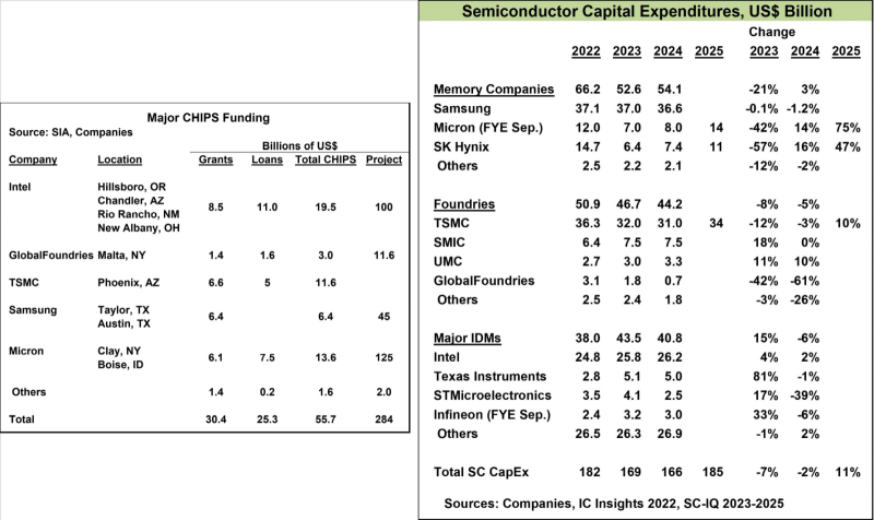
Left: Top recipients of US CHIPS Act grants and loans as of July 2024, showing cities and states where their factories are planned. Right: Capital expenditures of the world’s leading semiconductor companies in 2022-2023. plus an estimate for 2025, if available, in billion US dollars, as well as their year-on-year dynamics in % (source: Semiconductor Intelligence)
In the meantime, as CEO Pat Gelsinger said, although the Intel Foundry division’s revenue for the reporting quarter exceeded $4.3 billion, its operating loss reached $2.8 billion – and at least in the next quarter, and then these losses will only continue to accumulate longer. They are due precisely to the increase in the turnover of production lines according to the technological standards “Intel 4” and “Intel 3”, preparation for the start of serial production of chips according to the “Intel 20A” standard, as well as the continuation of work on the next technical process – “Intel 18A”, for which Already in July, the Process Design Kit was produced (a batch of pre-production samples, usually sent for testing to internal divisions of the company and/or partners interested in ODM production). As representatives of the chipmaker himself note, a significant contribution to the operating loss was made by more mature production lines (pre-EUV nodes), maintaining which in working order today requires considerable costs, while revenue from chips manufactured on them is steadily declining – since they are increasingly becoming cheaper. as new technological processes are developed.
Analysts warn that Intel’s intention to cut costs by cutting its workforce by 15% (about 15 thousand people worldwide) and cutting capital investments in order to free up about $10 billion could prove fatal to Mr. Gelsinger’s goal immediately after his Taking office as CEO, the goal is to achieve technological leadership in the microprocessor industry, displacing Taiwanese TSMC on this pedestal. The American company has already promised shareholders this year to reduce gross capital expenditures by more than 20% from the previous estimated value, thereby reducing them to $25-27 billion, and in 2025 to further reduce them to $20-23 billion. At the same time, the Taiwanese competitor Intel itself – apparently not so constrained by the expectations of shareholders in terms of redistributing profits to pay dividends (instead of long-term investments in production) – recently announced, as we mentioned at the very beginning, an increase in the cap on capital expenditures in this year from the previous 30 to 32 billion dollars. According to analysts from Semiconductor Intelligence, TSMC will continue to increase investments in capital goods in 2025 – by at least 10% of 2024 volumes.
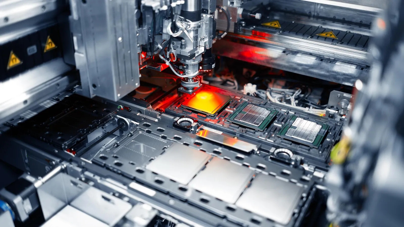
A machine for installing protective covers on composite chip packages intended for data centers at Intel’s plant in Chandler, Arizona (source: Intel)
And this, by the way, is not a reckless whim (after all, the burden of difficult macroeconomic realities does not fall on Intel alone – TSMC operates in approximately the same market and under comparable conditions), but a repetition of a strategy that has already justified itself once. During the financial crisis of 2008-2009, the founder of the Taiwanese chipmaker, Morris Chan, returned to the post of CEO – at the age of 77, by the way – against all obvious considerations, he increased the volume of capital investments, cutting dividend payments in return. This, according to many analysts, is precisely what contributed to TSMC consolidating its leading position in the global semiconductor industry. But it still has to defend its well-deserved leadership laurels: next year promises to be a time of intensified confrontation between chip manufacturers. Semiconductor Intelligence emphasizes that, although total capital investments in this industry at the end of 2024 will decrease worldwide from the level of 2023 by 2%, to $166 billion, in 2025 they will grow by 11% year-on-year – up to $185 billion, which will exceed the absolute peak of $182 billion achieved in 2022.
⇡#Hello, we are looking for talents
Another important point that experts from the Taiwanese publication DigiTimes pay attention to: Gelsinger’s ambitious plan to complete the five-year plan in four years – to master five successively increasingly miniature technological processes in just four years – encounters such a somewhat unexpected obstacle as the lack of the required number of specialists with the required qualifications. First of all, high-level professionals in the fields of R&D of semiconductor chips and their production technologies, of course; but not only them alone. For example, building the foundation, walls and ceiling of a new factory is not enough to begin mass production of modern VLSI chips there. The bulky and expensive High-NA EUV photolithograph requires a “clean room” with extremely tight tolerances for the content of dust particles in the atmosphere, and of a considerable volume. But for obvious reasons, there are not so many engineers, foremen and even workers in the world who are able and ready to create this kind of premises with guaranteed compliance with the standard, and the lion’s share of them is already involved in similar construction projects in Southeast Asia – where they are paid for So a serious struggle is already underway. For example, Samsung Electronics, according to the Korea Economic Daily, has begun a radical overhaul of its employee incentive system – precisely in order to stop the outflow of the most valuable engineering talent.
In theory, the Intel Foundry Services (IFS) division, in accordance with the IDM 2.0 strategy proposed by Gelsinger, should have become an internal talent forge for the parent company – by executing third-party orders, accumulating relevant experience and then applying it to produce the company’s own products. Intel. Let’s say, today chips of the Core Ultra family of the Lunar Lake architecture are produced entirely (and not in separate tile modules, as was previously practiced for Meteor Lake) not at American enterprises, but outside – using the “3-nm” technical process (more precisely, according to production standards N3B and N6) at factories of the same TSMC; simply due to the lack of suitable production lines at the disposal of Intel itself. In this way, the American chipmaker receives, if not direct losses, then a significant reduction in the profit margin, and therefore it was completely natural that he intended to manufacture the next generation of processors, Nova Lake, – already in 2026 – at his own (not yet built) enterprises, and at the same time and using significantly more advanced “Intel 14A” technology. However, in early August, information began to arrive from sources close to Taiwanese semiconductor circles about a change in Intel’s priorities: TSMC will continue to remain the main manufacturer of Nova Lake chips, while the American chipmaker “will continue to study the development of its own developments in the field of “14-Å” production standards.” , choosing the right moment to switch from ordering new processors from an ODM partner to releasing them on domestic lines.
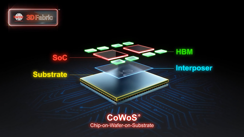
Chip-on-Wafer-on-Substrate (CoWoS) technology proposed by TSMC allows the distance between individual chiplets within a composite chip to be reduced to 0.03 mm – compared to the minimum of approximately 20 mm that is required, for example, when mounting the computing core separately and HBM memory (source: TSMC)
To be fair, it is worth noting that IFS already has its own external customers – AWS, Qualcomm, Microsoft, and more recently NVIDIA, which found the capacity of the CoWoS packaging lines at TSMC factories to be insufficient due to the explosive growth in demand for its “ graphic” (more likely “neural”) chips for training and executing generative artificial intelligence models. The advanced technologies for packaging composite, including vertically integrated, CoWoS (TSMC) and Foveros (Intel) chiplets into a single package are in many ways similar, which allows large customers like NVIDIA to effectively distribute the load between available production lines. But still, the packaging of chips, even the most sophisticated one today, is not as profitable as their manufacture according to the most advanced technological standards – and therefore IFS will continue to remain a low-profit enterprise until it masters the confident production of at least “3nm” (recall that the “Intel 3” process technology in TSMC terminology is closer to “4-nm” than to “3-nm”) VLSI.
Meanwhile, TSMC, objectively being in a better position compared to Intel precisely as a manufacturer of microcircuits (it itself, let us remind you just in case, does not develop them, acting precisely as an ODM partner for their production for external customers), continues to confidently collect coupons against the background the slow recovery of the global semiconductor market, primarily due to the growing interest of customers in AI-oriented computing systems. In July of this year alone, the Taiwanese chipmaker earned more than $7.9 billion – 23.6% more than in the previous June, and 44.7% more than in July 2023, thereby updating its absolute record monthly revenue and exceeding analysts’ wildest expectations for second-quarter financial results. A further increase in income is expected based on the results of the third quarter. — From July to September, TSMC plans to generate revenue from $22.4 to $23.2 billion, which corresponds to a quarterly increase in the range of 7.6-11.4%. At the same time, experts estimate its gross profit at an impressive 53.5-55.5% of revenue, and its operating profit (gross minus operating costs) at 42.5-44.5%. It is not surprising that TSMC is actively building new factories: in addition to the Japanese and American branches already under construction, the foundation stone for the subsidiary European Semiconductor Manufacturing Company (ESMC) in Dresden, Germany is scheduled to be laid at the end of August.

Through-holes, made in a single pass in a semiconductor chip on a 0.55 NA EUV photolithograph, are located extremely tightly (the minimum distance between their centers is 30 nm) and in exact accordance with the intended pattern (source: ASML, Imec)
So while Intel is selling its stake in the developer of processor architectures Arm in an effort to minimize losses, its fellow competitors in mastering the most advanced technological processes are actively increasing their momentum. And it’s not just Taiwanese and South Korean companies that rely mainly on the same off-the-shelf EUV photolithographs from ASML as Intel itself, which in the most recent High-NA version (with a numerical aperture of 0.55) now allow semiconductor manufacturing in a single pass. crystals with through holes at distances of 30 nm between their centers, as well as perform topological structures (transistor elements and their interconnections) with characteristic dimensions of no more than 9.5 nm with a pitch between them of 19 nm. In the last few months, the Japanese have also actively joined this race: in addition to creating a Canon nanoimprint lithograph, the Okinawa Institute of Science and Technology managed to significantly simplify the optical design of a standard EUV machine, making do with only two mirrors instead of six. If we take into account how significant the energy losses are during multiple reflections of a photon beam, a two-mirror photolithograph brought to readiness for serial production will be able to provide the chipmakers using it with a significant reduction in production costs – and thereby a dramatic gain in the cost of finished microcircuits.
⇡#Give me two!
The American CHIPS Act, which guaranteed total subsidies (in the form of grants and loans) of almost $56 billion to semiconductor manufacturers building factories in the United States, is far from the only program of its kind in the world. The previously mentioned researchers from Semiconductor Intelligence indicate that the European Union as a whole is concerned about the development of the microprocessor industry in its territories (the volume of its similar program is $46 billion), Germany separately ($21 billion), South Korea ($55 billion; however, only in the form of tax breaks), Japan ($25 billion), Taiwan ($16 billion), India ($10 billion) and, of course, China — $142 billion.
However, from the point of view of the fastest and most successful development of technological processes of the “2nm” class, the main competitors in the global semiconductor arena will, of course, be Intel with its production standard “Intel 20A/18A” and TSMC with N2/N2P processes. The readiness of the N2 technical process for mass production of chips in 2025 has already been announced; N2P will become closer to the second half of 2026 with its evolutionary development, ensuring the productivity of finished products increased by approximately 5% and their energy efficiency improved by 5-10%. Confident reports from TSMC representatives about maintaining the planned pace of N2 development make experts doubt that the Intel 18A, when it reaches the mass production stage in 2026, will be able to become, in the eyes of potential customers, a desirable alternative to the N2/N2P options offered by TSMC – although more A “rough” version of this production standard, “Intel 20A”, should appear from the American company before the Taiwanese one.
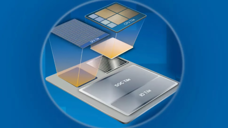
Anatomy of a composite “2nm” Arrow Lake processor (source: Intel)
The Foundry 2.0 concept, announced in July, promises to give additional impetus to the further development of TSMC – adopted not so much in defiance of Intel’s IDM 2.0, but clearly taking it into account. The Taiwanese chipmaker strives to become for its customers not just a custom VLSI manufacturer, but a full-cycle semiconductor manufacturing service provider – from the preparation of lithographic masks to packaging and testing of finished chips. As of Q1 By 2024, TSMC accounts for 61.7% of all revenue from global contract manufacturing of chips, and with the implementation of Foundry 2.0, this company expects to cover at least 28% of the global semiconductor industry as a whole (also in monetary terms) with its offerings.
It is interesting, by the way, that the leading Taiwanese chipmaker continues to rely on EUV photolithographs not of High-NA, but of the previous generation, which are more budget-friendly and largely paid for themselves at the stage of mass production of “5-nm” microcircuits – which provides it with an additional advantage in compared to Intel, which is already purchasing the second ultra-modern machine of this class from ASML. According to DigiTimes sources, TSMC intends to massively purchase the corresponding equipment already at the stage of mastering the A14P process technology (approximately the same “1.4-nm” category as the “Intel 14A”) only in 2028, and until then it will continue to mostly make do with less advanced machines. Which, from an economic point of view, again puts Intel at a disadvantage – since the American chipmaker will have to return capital investments in fresh production equipment in the coming years, which will limit its ability to maneuver prices on the open market.
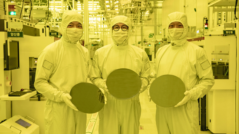
South Korean microelectronics manufacturers proudly demonstrate photolithographed wafers with “3-nm” VLSI based on GAA transistors – and are confident that in about a year they will also be able to show “2-nm” products of their own production (source: Samsung Electronics)
South Korean Samsung Electronics has chosen its own special path to “2 nm,” which also declares its readiness to launch mass production of “2 nm” chips in 2025. It should be borne in mind that the “3nm” technology mastered by this company (formally the first in the world) is not particularly popular among customers: in fact, the only major customer of such chips from the South Korean manufacturer is System LSI, its own division, engaged, in particular, in the design of Exynos system-on-chip. Experts call the reason for such a restrained attitude of customers towards a seemingly reasonable alternative to TSMC, which currently reigns supreme in the “3nm” segment, the devastatingly low percentage of yield of usable chips made according to this production standard on Samsung Electronics lines, which is why the cost of finished ones ( and accepted by the customer) of products turns out to be higher, and the agreed delivery dates may be significantly delayed.
Nevertheless, the South Korean chipmaker has nowhere to go: while its position in the memory chip market (both DRAM and NAND) is quite strong, in the logic chip segment it lags significantly behind both TSMC and Intel – and this is where we can hope to to the high margins of semiconductor production, driven by significant demand for hardware for AI computing. Strictly speaking, high-speed HBM RAM for graphics and neuro accelerators is also a very profitable product, and Samsung Electronics successfully supplies it to the same NVIDIA. But since the production standards for memory chips in terms of miniaturization are noticeably inferior to those for logic VLSIs, competition in this area is significantly higher – and the margins are correspondingly lower.
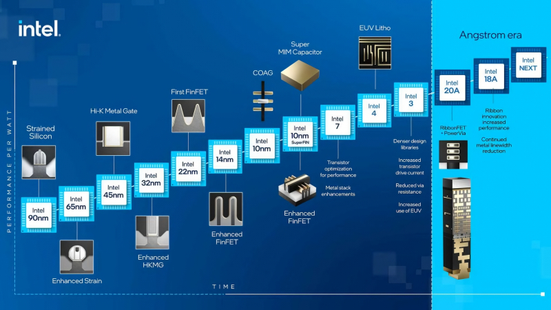
Stages of improvement of microprocessor technologies as technological standards for VLSI production are miniaturized (source: Intel)
So, the South Korean chipmaker – more precisely, its semiconductor division Samsung Foundry – intends to immediately occupy an advantageous position in the as yet non-existent segment of custom “2-nm” microcircuits, developing an appropriate technical process based on transistors with Gate All Around (GAA) gates. and thereby realizing its advantage – obtained, however, at the cost of lagging behind the Taiwanese leader in points in the currently relevant “3-nm” standings. GAA transistors are already being used by the South Korean company in the first generation of its “3nm” chips – and, as we already discussed in one of the “semiconductor cycle” articles, they do seem to be a very promising choice for even smaller production standards. True, their technical advantages – lower heat loss when a charge passes through the gate, increased energy efficiency – are largely offset by purely technological difficulties in establishing their mass production with an acceptable high percentage of yield of suitable products. TSMC and Intel also intend to switch to NanosheetGAA and RibbonFET transistors – respectively, in the course of mastering the N2 and Intel 20A/18A technical processes. However, taking into account the experience Samsung Foundry has already gained in working with GAA, the South Korean chipmaker has considerable chances to gain an advantage here, even if only temporarily.
In turn, Intel recently confirmed its intention to begin serial production of Arrow Lake architecture processors before the end of this year – although earlier industry experts expressed concerns that against the backdrop of a forced reduction in capital investments, recording quarterly losses and the postponement of the Innovation 2024 event, the American chipmaker would postpone the launch of the first chip of this class, which will be manufactured, as expected, using Intel 20A technology. Thus, formally – if the planned release does take place in 2024 – Intel will be ahead of both Taiwanese and South Korean rivals in mastering the so-called “2nm” segment. Although we should not lose sight of the example of the same Samsung: even though it was the first to start mass production of “3-nm” VLSI, the cream of the order from microcircuits using this technical process is precisely for the reason already mentioned for the too low share of usable GAA- chips on each photolithographed wafer – TSMC still removed it: a little late, but relying on FinFET structures that were perfectly debugged in production.
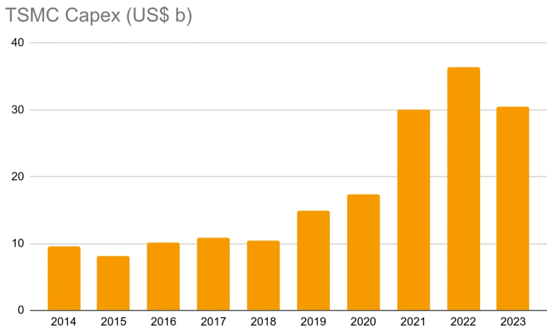
TSMC capital expenditures by year, billion US dollars (source: Bloomberg)
TSMC itself, by the way, is serious about maintaining global leadership in the “2nm” race. According to DigiTimes, the company is systematically preparing for the transition to a new technological process in 2025 and beyond at least six of its factories in Taiwan alone, and the Arizona enterprise of the Taiwanese chipmaker, scheduled for imminent commissioning, will also specialize first in “2-nm” , and then on “1.4nm” chips. In total, by 2025, ASML is going to supply TSMC with 60 EUV photolithographs (not High-NA for now, remember), mainly for “2-nm” lines, for a total amount of $12.3 billion.
However, unlike the “3nm” competition, when it was quite easy for the Taiwanese chipmaker to bypass the South Korean one who made a false start, this time the strengths and capabilities of both of its leading rivals are very great (plus, let’s not forget about the growing Japanese semiconductor manufacturers) – despite all the objective factors playing against them. Therefore, if the demand for high-performance hardware for AI computing continues to meet the bold forecasts of analysts, there is no doubt that all available “2nm” production capacity will be fully loaded with orders as they come into operation, including from competing vendors – to the delight of us, the end consumers.
Related materials
- Samsung produces chips for external customers at a loss.
- The Japanese Rapidus, through automation, expects to significantly speed up the execution of orders for the production of 2nm chips.
- Imec created record small semiconductor structures in a single pass using High-NA EUV.
- Intel boasted of its success in mastering the 1.8-nm process technology for itself and contract customers.
- Intel will soon install a second ASML lithography scanner with High-NA EUV – it will produce 1.4 nm chips.
- Production of Samsung Exynos 2500 will start in the second half of the year – the chip may end up in Google Pixel.