Manufacturers of RAM chips, following the example of their colleagues from the logic chip segment, are introducing the use of EUV lithography, but this leads to increased costs. To justify it, according to representatives of SK hynix, memory chips need to be switched to using a vertical arrangement of transistors, and then the actual cost of memory will even decrease.
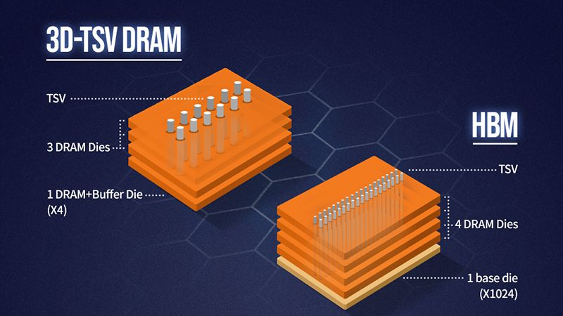
Image Source: SK Hynix
The corresponding comments by Seo Jae Wook, who is responsible for scientific research at SK hynix, are given by the South Korean resource The Elec. The classical approach to the use of EUV lithography in the production of memory chips, according to him, can hardly be considered rational from the point of view of its impact on cost. But if you switch to using transistors with a vertical arrangement (VG or 4F2), then the area of the memory crystal can be reduced by 30% compared to the classic 6F2 technology, and in combination with EUV, this arrangement will reduce costs by half.
Samsung Electronics is also considering the possibility of producing so-called 3D DRAM with “vertical” transistors, like SK hynix, this company expects to use technological processes with standards of less than 10 nm. The RAM industry can no longer rely solely on planar transistor packaging, since the implementation of EUV equipment in this case becomes unreasonably expensive. But in combination with a new transistor structure, the introduction of EUV lithography can justify itself, as representatives of SK hynix note. However, the introduction of a new transistor layout will require the use of not only new equipment, but also new materials in the production of DRAM chips. Most likely, the technology will take root in mass production no earlier than 2027. Samsung intends to introduce multi-layer DRAM in the next decade.