Among the foreign applicants for funds under the “CHIP Act” in the United States at one point was the South Korean company SK hynix, which in April of this year announced its intentions to invest $3.87 billion in the construction of a memory chip packaging plant in Indiana. The company has now reached an agreement to receive financial support from the US authorities for the implementation of the project.
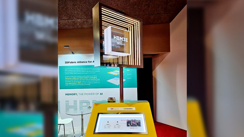
Image Source: SK Hynix
Formally, as noted in the official statement, the agreement is preliminary, but the company already expects to receive from the US authorities not only $450 million in non-repayable subsidies, but also preferential loans in the amount of $500 million, as well as the right to a 25 percent tax deduction, which will be extended for SK hynix’s capital expenditures for the construction of its Indiana facility. Before funds are allocated, SK hynix will have to undergo verification of compliance with the conditions for providing such benefits.
It is specifically emphasized that the Indiana facility will serve the purpose of meeting the demand for memory for the artificial intelligence segment. Accordingly, at this site SK hynix will package HBM type memory of current generations in order to supply it to Nvidia. If the latter can entrust the production of specialized chips to the American enterprises TSMC, then in fact completely finished computing accelerators can be produced in the USA. In any case, reducing dependence on Asian plants for American chip designers will be a favorable outcome of the construction of the SK hynix facility in Indiana. The company is also going to train personnel for this plant with the involvement of the local Purdue University.